 BaumInventions
Chapter 0 : Bla...
For me it is really important to understand things. If i make, build or research something i try not just to take a already existing solution. I like to take my own notes, make my own thoughts and probably waste a lot of time doing things twice... BUT it will stay in my brain and create a base of knowledge to build on.
Writing about things helps a lot to sort the thoughts and decide wich informations are relevant to keep.
What you will find here is a collection of notes and thoughts that will help me understand as much as possible about the Texas Instruments speech synthesis found in Renault synthesizer boxes. My imaginary goal is to preserve the ROM data of the increasingly rare synthesizer boxes and maybe use the same type of speech synthesizer IC in a standalone application where a modern Microcontroller is used to control the speech synthesizer AND simulate a ROM to the synthesizer. I know there is already a full emulator of the Texas Instruments Speech... But wouldnt it be nice to use a piece of real 1980s electronics?
Chapter 1: Used Hardware
The Speech Synthesizer used in the boxes is a Texas Instruments TMS5110A (Datasheet of TMS5100 wich is pin compatible) in combination with a special ROM called TMS6100(Datasheet). This ROM is a very special part. It has its own very strange way of communicating to the speech synthesizer. Lets start with a look at the PINOUT of both IC´s. I wanted to see the IC´s directly next to each other and so i made this handy little picture:
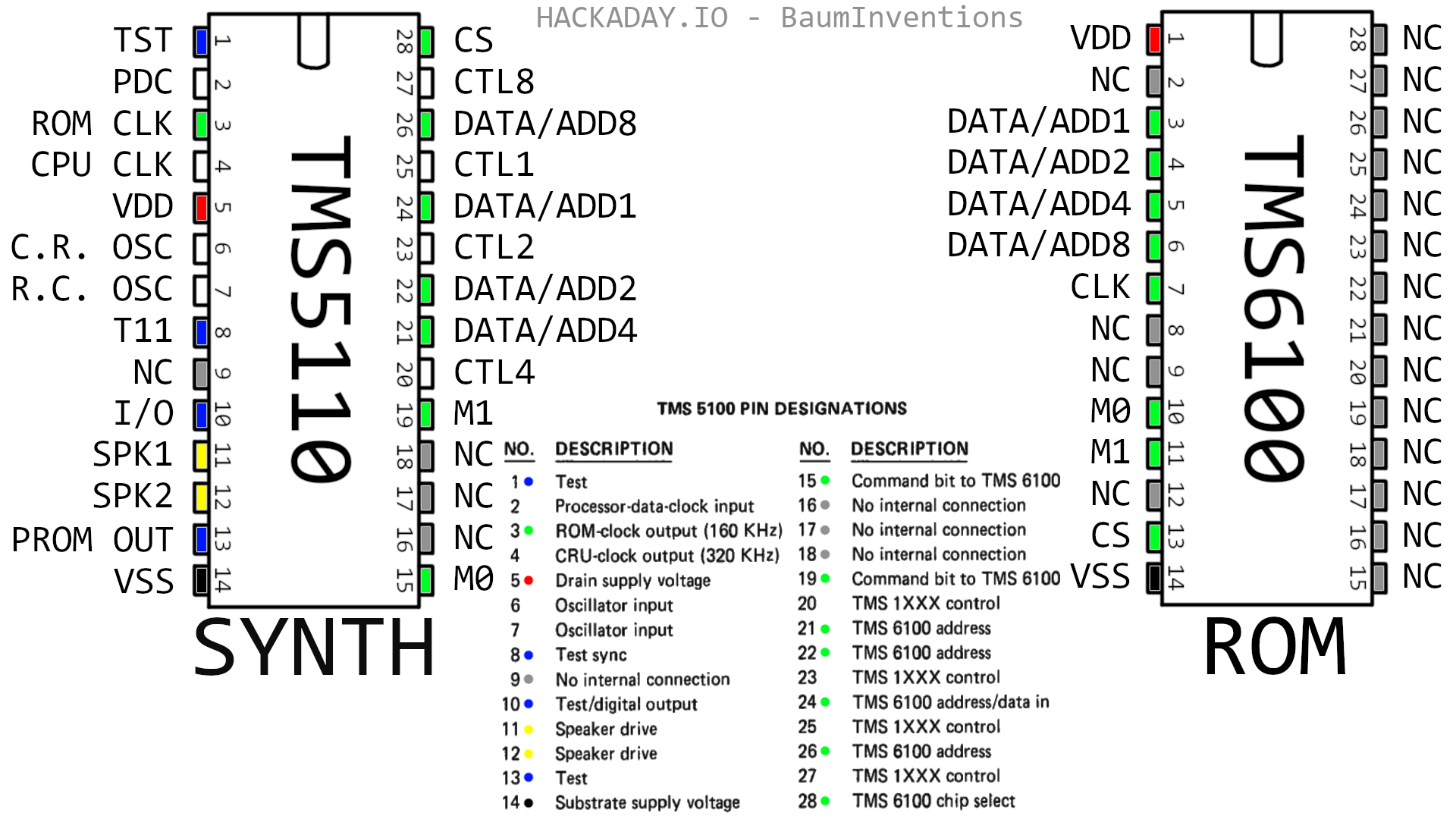
At the first look you will probably ask yourself why the ROM has so many unused (NC) PIN´s (marked in GREY). And the answer is: I don´t know... For me this looks like a waste of material. But there will be a reason... i guess... The reason is probably not to make connecting it more easy. The corrosponding PIN´s on the TMS5110 are in a totally different order so you always have to route your PCB traces in a strange way... All the 8 used PIN´s from TMS6100 are directly connected to TMS5110. I have marked all directly connected PIN´s used by the ROM GREEN.
Later we will see that they are "using" the unused pins to just route signals "through" them. It is important to know that the NC Pins on the ROM (and synth) are really NC inside the chip! If we want to replace the ROM with something else we have to make absolutely sure the NC PIN´s of our solution are really NC! Dont make the mistake like me and think "because a trace goes through that PIN it must be relevant for the circuit." Because its not.
If you are easyly distractable like i am here is some trivia for you: The ROM they used has a gigantic capacity of 16 kilobytes. This may sound like nothing today but back in 1983 when they made this thing it was quite a lot. Let´s compare it to the Atari 2600 wich was sold around the same time. The Atari had 128 BYTES of RAM and a whole Game was around 2-8 kilobytes. Commodore put gigantic 64 kilobytes of ram in the C64 and this was A LOT at that time. Commodore wanted to rival the Apple 2 wich had 4 - 64 kilobytes of ram at that time. You can see that the 16 kilobyte ROM was probably the most expensive part. And now to distract you even more lets watch half an hour of computer chronicles from 1983 about revolutinary storage devices like "Hard Disks" wich slowly started to shrink from compact car sizes down to shoe Box sizes...
The next thing we should talk about is the supply voltage(marked in RED and BLACK)... It would be too easy if they just used a regular voltage. So they decided to use 9 Volts NEGATIVE. 9V are not just pretty high for modern standards but also its negative. But lets not focus on that little detail... later its getting even harder...
Another pretty interesting detail are the TEST PIN´s (marked in BLUE). There are 4 dedicated PIN´s just for some kind of testing purpose. At the time of writing this i have no idea how to use them... if they even do something.
Lets explore all the PIN´s on real hardware to see the implementation.
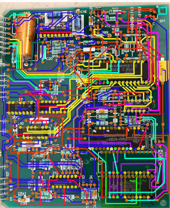
Don´t worry... it looks more complicated than it is. Our main focus is the bottom right corner.
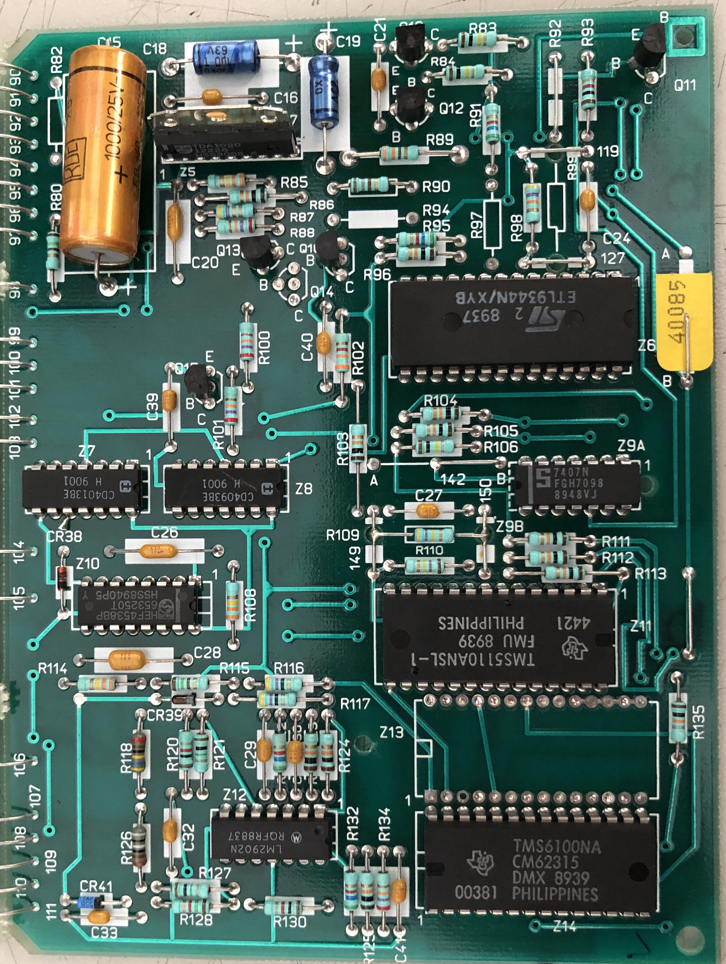
On the bottom right you see "Z14" and "Z13". Z14 is populated with our TMS6100 ROM. Z13 could be populated with another ROM but is left empty from the factory. "Z11" is the speech synthesizer TMS5110A. Both ROM sockets are wired in parallel to the synthesizer, like we have seen on the pinout of the chips. If you scroll up to the traced version of this picture you may notice that the CS (Chip Select) pins of both roms are not wired in parallel to the TMS5110. Texas Instruments had intended to give each chip its own ID. So all roms could be wired in parallel. Each ROM would be only accessable if the right ID is sent. But here the Microcontroller "Z6" on the upper right side is generating the Chip Select signal. One Pin of the Microcontroller (PIN 28) is either HIGH or LOW and drives a transistor wich selects either ROM to use.
WORK IN PROGRESS!!
private notes:
write about cs...
write about unused pins...
write about microcontroller connection.
write about clock generators
write about voltages.
---
next: protocols / communication
Discussions
Become a Hackaday.io Member
Create an account to leave a comment. Already have an account? Log In.