The story behind this project
Every now and then I would find the need for a differential probe. I’d end up using a high voltage diff probe, which you've probably seen lurking around most electronics labs – the ones housed in a large rectangular box with a pair of heavy leads dangling out one end. While great for high voltage work, they were a hassle for general purpose measurements. Those giant leads are not a good match for probing small components. Their high attenuation levels resulted in noisy measurements at lower voltages. I was always left wondering if I could trust higher frequency measurements, with the leads dangling between the probe and device under test and flopping onto the PCB.
That got me thinking . . . is there a decent smaller probe out there to add to my lab? Could you use something like it too? It turns out that the big name test equipment companies have some really nice diff probes, many exceeding 100MHz bandwidth. However, the prices start in the thousands, and often have a brand-specific interface.
So, I figured, it can’t be that hard to build one and started reading up on how they work. Armed with modest goals and a little knowledge, I went about designing a simple 10 MHz-ish probe. It seemed very doable . . . but then I thought, 100MHz bandwidth would be nice, or maybe a little more. Things got harder, but maybe still doable. It would also be nice to get rid of the potentiometers and other annoying adjustments that you need to get good common mode rejection and DC offset and so on. Oh, and it would be nice to have an insulated enclosure. Now the design was getting tricky and I got bogged down. A little more scope creep later, this project was born!
HACKADAY project goals
Many months and iterations later led to what you see in the project photos. It suits my diff probe needs for now, so what next? I figured I would get the design out there, so you could build it if you’d like. Or if there’s enough interest, iron out some of its rough edges and make a product of it. I’m happy to hear your feedback, so feel free to comment.
Specs & features at glance
Okay, so that’s all well and good, but what can this thing do? I did my best to balance cost and complexity and came up with the following specs and features. So without further ado, here they are:
Specs:
| Bandwidth, 3 dB | ≥150 MHz |
| Attenuation | 20:1 |
| Differential signal range | ±20 V |
| Common mode range | ±30 V |
| DC offset voltage | ≤ ± 10 mV, referenced to input, after zeroing |
| CMRR, 60 Hz | ≥ 70 dB, referenced to input |
| CMRR, 10 MHz | ≥ 40 dB, referenced to input |
| Input Resistance, between inputs | 1.08 MΩ between inputs, 540 kΩ from each input to ground |
| Input Capacitance at 10 kHz | ≤ 3 pF between inputs, ≤ 6 pF from each input to ground, typical |
| DC Attenuation Accuracy | ≤ ± 5% |
| Pulse Rise Time (10% to 90%) | ≤ 2.4 ns |
| Gain Flatness, 0-30 MHz | ≤ ± 0.5 dB , typical |
| Input Damage Threshold | 100 V |
Features:
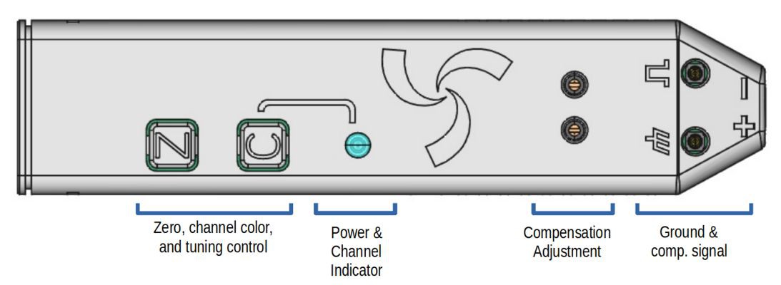
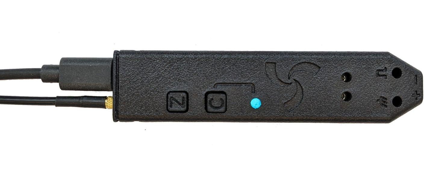
LED scope channel indicator: This helps you keep track of what scope channel the probe is connected to, especially if you're
using more than one diff probe for a test. PD150's LED color can be set
to any standard scope channel color. Use the "C" button to cycle
through colors.
- Flexible probe interface: The probe inputs are simply 0.1-inch spaced sockets. Their close spacing is good for measuring higher frequency or sensitive signals. You can solder a header to the circuit to connect to. For less critical work, you can attach jumper wires.
- USB Power: PD150 is powered through a USB-C connector. It needs 5V at 300 mA, which can be provided by a small adapter or many USB ports.
- Scope compatibility: PD150 has a BNC signal cable and 50 Ω output impedance. Thus you can connect it directly to a scope with a 50 Ω input, so long as its rated for at least 2.5 Vrms. For scopes with only a high impedance input, you can use a 50 Ω inline attenuator between the probe and scope.
- Automated low frequency common mode rejection adjustment: Its nice to have a really high common mode rejection at low frequencies. This basically means that both inputs are near perfectly balanced in attenuation. So if you're measuring a small signal that's riding on top of a larger noise source, such as 60 Hz line frequency noise, the noise will get subtracted out, allowing your signal to be visible. This is a very finicky adjustment which would normally need to be done manually with a trimmer potentiometer and a pile of test equipment. PD150, automates this adjustment using a built in test and measurement features. All you need to do is connect a jumper and activate the adjustment feature.
- Automated DC bias tuning: Like many active probes, the DC offset can drift over time, causing a slight DC offset in the output. In other words, if you apply 0 V to the input, a non-zero voltage appears at the output. You can eliminate this offset by pressing the "zero" button. It will automatically correct the offset to 10mV or less.
- Compact size: PD150 is compact and easy to hold in your hand. It measures 10 x 2.4 x 1.5 cm
- High damage threshold: The inputs can tolerate up to 100 V to ground, so you can probe around lower voltage circuits without worrying about destroying the probe.
Diff probes - why and when to use them
Alright, with all the specs and features out there, we can dive into the interesting part - the probe design. But hold on, if you're new to diff probes, you may want to read below for a summary of what diff probes are and when you need one.
It helps to first think about how you use a regular passive probe. Its probe tip is high impedance, which is great since it won't short or load down a circuit node (within reason). But the second terminal that you need to connect - the ring or clip - is not so friendly. It connects to the scope chassis, and in turn to the clips on all the other probes, along with earth ground through the scope's receptacle. Thus it can load things down and short parts of your circuit. So you can't go connecting those clips willy-nilly!
Despite their limitations, passive probes are usually fine. But sometimes you can't find a suitable spot for those ground clips. Perhaps you need to probe the voltage across an inductor in a buck converter, or test a differential interface. This is where diff probes shine. Both of their inputs are high impedance. Thus you can probe away across various points in a circuit without worrying about shorting various points together.
If you're interested in further learning on the topic, w2aew has a very helpful video: #74: Basics of Differential Probes for Oscilloscopes and their applications: a tutorial
Design goals
Aspirationally, I wanted to meet the performance (voltage and bandwidth) and convenience of a standard passive probe, but in differential form. This would meet most of my testing needs, and hopefully for you too. Here's what I came up with as a rough set of design goals.
These goals are fully met by the current prototype:
- At least 100 MHz bandwidth
- Handheld probe or probe head that can get close to what you're measuring (for convenience and reproducible measurements)
- Relatively affordable - BOM cost of not more than about $100 for moderate quantities
- Good gain flatness. Helps with trustworthy high frequency measurement
- Input voltage damage threshold of at least 100 V
- Generic scope interface that can be used with most scope models
- Insulated enclosure - don't want to short out circuits with the probe body
- EMI shielding to avoid measurements being corrupted by nearby fields
- Low attenuation (for lower noise), ideally 10X. The prototype is 20X
- Channel indicator. Useful when using multiple probes
These goals were partially met by the current prototype:
- Automated adjustments - less effort needed to perform adjustments. The prototype has three adjustments, of which two are automated.
- Documented performance verification. Useful if you want to calibrate the probe on your own. This is still in progress
- Powered through a USB connector - no need for a specialized power adapter. The prototype is powered by USB and works on most ports. However, it lacks USB enumeration and support for the full voltage ranges that could be encountered.
- Comprehensive documentation with theory of operation. I'm a fan of old school test equipment manuals. This is a work in progress.
These goals were not met:
- Differential mode range of +/- 30 V. The prototype's range is +/-20V due to slew rate limits at its maximum operating frequency.
Theory of operation
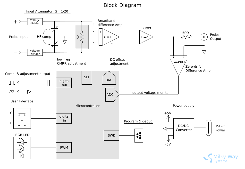
This section describes generally how the probe works. I'll refer to the block diagram below. It's a birds eye view, showing all the probe's subsystems, but without much circuit detail.
The signal path:
This section describes how an input signal makes its way from the probe's inputs to the output.
It all starts out with the probe's positive and negative inputs shown at the top left of the block diagram. The voltages applied to each input are attenuated by a factor of 20 (or gain of 1/20) by two identical voltage dividers. This keeps the active components downstream within their allowable input voltage ranges. You'll note there are also some adjustable components following the voltage dividers. We'll ignore those for now.
Next, the attenuated signals are input to a difference amplifier - the core of the differential probe. It subtracts the two signals. Its output is thus equal to the voltage difference being probed, scaled down by 1/20. Any so called common mode voltage appearing at both inputs is eliminated. This is what makes the probe differential.
Finally, the signal is buffered so it can drive the scope's 50 ohm input. The buffered signal goes through a 50 ohm resistor before exiting through the output connector. This 50 ohm resistor terminates the source end of the coaxial cable. The opposite end of the cable will be terminated in 50 ohms by the oscilloscope's 50 ohm input. In this scheme, the coaxial cable is terminated at both ends in 50 ohms. This both minimizes signal reflections and ensures that the probe's buffer sees a consistent impedance (of 100 ohms) at its output through all frequencies. Both help maintain a flat frequency response. These two 50 ohms resistors form a voltage divider, halving the voltage. The buffer's gain of two cancels out this loss.
DC offset adjustment:
When you apply zero volts across the probe's inputs you'd expect the same at the probe's output. However, the signal path described previously doesn't do a great job of it. The reason is that most broadband amplifiers necessary for the probe's bandwidth have poor offset voltage specs. Also, any DC error will be multiplied 20x by the oscilloscope to match the probe's attenuation. For instance, a small error of 5 mV in the signal path would appear as 100 mV on the scope's screen! Thus we need a way to reduce the DC error.
The PD150 cancels the DC offsets by injecting an offset of opposite polarity into the signal path. It's activated by pressing the "0" button on the probe with the inputs disconnected. This button is shown under the user interface section of the block diagram.
The DC offset correction voltage is applied to the broadband difference amplifier. Look closely and you'll see it has a third input. It is labelled ref (short for reference) and shifts the DC level of its output. This is coupled to the microcontroller's DAC so that the adjustment can be automated.
The microcontroller will need to monitor the probe's output voltage to know what correction voltage is needed. The tricky thing here is that it'll need to detect when the output crosses zero volts to within 500 uV to meet the spec. The reason for the stringent value is the 20x multiplication factor described above. A zero-drift amplifier, shown on the right side of the block diagram, helps out here. It has excellent DC performance and a lot of gain. That way the microcontroller does not need to detect tiny voltages that could be skewed by ADC quantization and its own offset errors. The zero-drift amplifier's output feeds into the microcontroller's ADC.
High frequency compensation:
At low frequencies, the probe's attenuator uses precision resistors to divide the input signals by 20, and this works quite well. At higher frequencies, the signals take a different path through a capacitive divider, for reasons we'll get into in the detailed circuit description. While resistors are readily available at 0.1% tolerance, precision capacitors aren't really a thing - a tight capacitor tolerance might be 5-10%! Plus, at the low values we're dealing with, various parasitic capacitances on the PCB and probe connector are very significant anyhow. So we certainly can't rely on capacitor values alone to get an accurate attenuation.
To remedy this, the probe uses a pair of tuning capacitors to adjust the capacitive dividers. They are shown in the block diagram to the right of the voltage dividers and labelled HF Comp (short for high frequency compensation). These capacitors can be adjusted to achieve a good 20:1 attenuation at both inputs.
You adjust them similarly to how you compensate a passive probe, by applying a square wave and turning the compensation capacitor till you get a proper response. The probe even provides a square wave output on its compensation and adjustment output (bottom left side of the block diagram). This output uses a digital output on the microcontroller to generate a fast rise time square wave.
Low frequency common mode rejection ratio adjustment
It's nice having very high common mode rejection at lower frequencies. For instance, you might want to measure a small signal that's sitting on top of higher amplitude 60 Hz line noise. If the 60 Hz noise is common to both points being measured, the probe cancels it out, revealing the small signal you're looking for. Meeting the 70 dB CMRR (common mode rejection ratio) in the specs requires the attenuation of the two voltage dividers to be exceptionally well matched to each other. Even better that the 0.1% precision resistors used in the circuit can guarantee.
Given this issue, we'll need an adjustment to better match the attenuators. Most probes use a manual trimmer potentiometer to do so. You'd carefully adjust this potentiometer with the probe hooked up to a signal source. I wanted to avoid it all costs because it is a very tedious thing to adjust. Instead, PD150 uses a digital potentiometer (aka digipot) for the tuning. It's shown just in front of the difference amplifier's input in the block diagram.
To automate the adjustment, we'll need to apply a common mode test signal to the probe inputs. The probe's microcontroller has us covered here! It'll generate such a signal on the compensation and adjustment output using a digital output. It needs to be connected to both probe inputs using a jumper cable with three pins.
The microcontroller will also need to monitor the output voltage while adjusting the potentiometer. It'll have to tweak the setting to minimize the probe's output voltage. The hard thing here is that the microcontroller must be able to see some exceedingly small output voltage changes to make a good adjustment. Here it gets help from the zero-drift difference amplifier connected to the probe's output. It boosts the probe's output signal and passes it along to the microcontroller's ADC.
All of this is activated through the probe's user interface switches at the bottom left of the block diagram. Putting it all together, the first step is for the user to connect the compensation and adjustment output to both probe inputs with a three pin jumper cable, then press the appropriate button combination to run the adjustment routing. The microcontroller takes over from there. It will measure the output voltage while adjusting the potentiometer and find the optimal setting. It stores the setting in nonvolatile memory.
Performance testing
I've needed to do a ton of testing to verify the probe's performance. This section summarizes some of the test results that I've gathered thus far. I've posted more details on testing in the project logs.
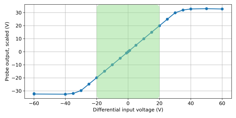
Differential voltage range
This plot shows PD150's response to a DC differential input voltage ranging from -60V to +60V. Note the linear response when operating within its ±20V specification. This region is highlighted in green.
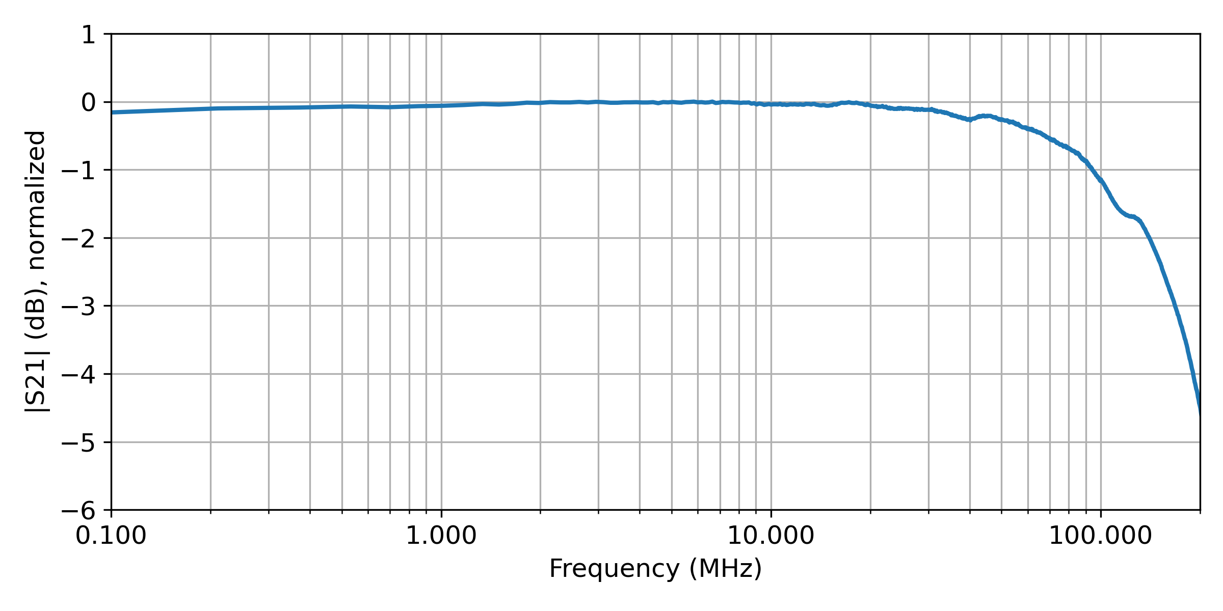
Frequency response
The following plot shows PD150’s typical frequency response in a 50 ohm system. I was measured using a vector network analyzer with a 50 ohm resistor placed across the probe's input.
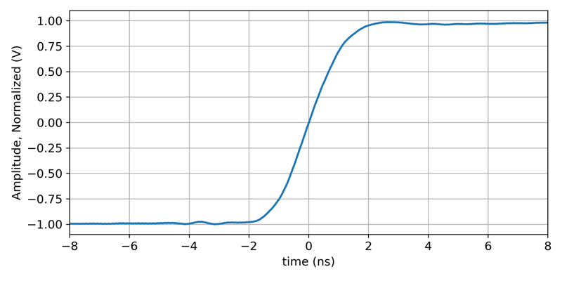
Differential Pulse Response
PD150’s response to a differential pulse is shown below. For this test, a high speed differential pulse with an amplitude of approximately 2V peak to peak was applied to the probe input.