 mkdxdx
Now that boards have arrived, time to soup up the indication panel with something a bit less messy.
The new board is to the left.
Board archive for instant JLCPCB quote will be added to file archive. You will also need new spacer panel which receives PCB bolts and is tied to the case with large power switch nut.
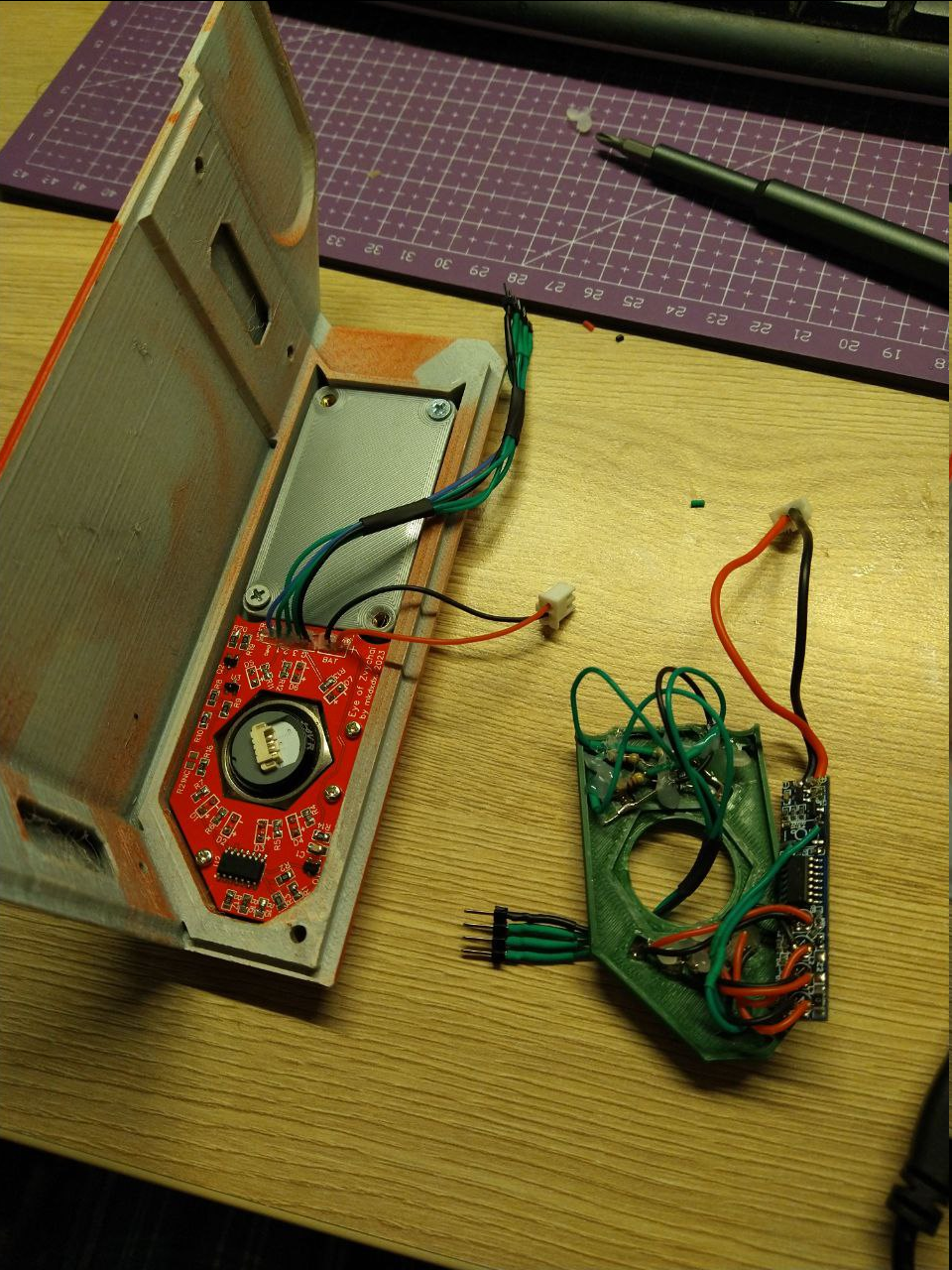 The only problem with it is that i have used PH2.0 connectors to interface the board with everything, and even they have high enough profile to push against battery caddy and prevent top cover from being flush when assembled.
 So for now i will not use PH2.0 connectors and just solder power and interface wires directly and apply some sauce to add strain relief - after all you absolutely do not want your battery terminals to break off easily and fly around within enclosure to cause high octane havoc. Maybe i will release another board revision that has connectors moved to the top part so they won't press against battery caddy since this is more safe.
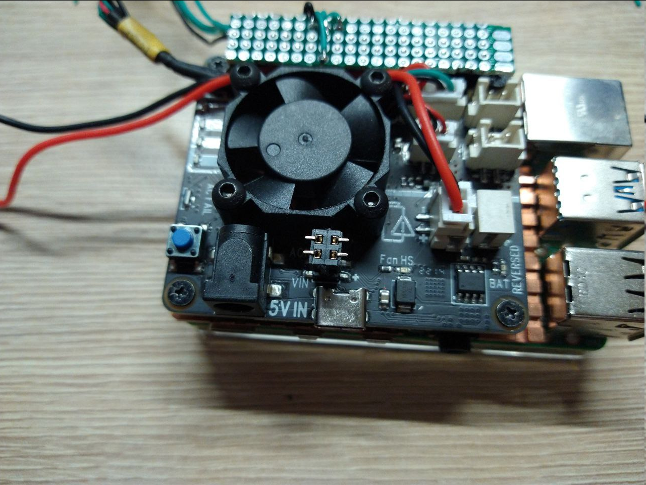
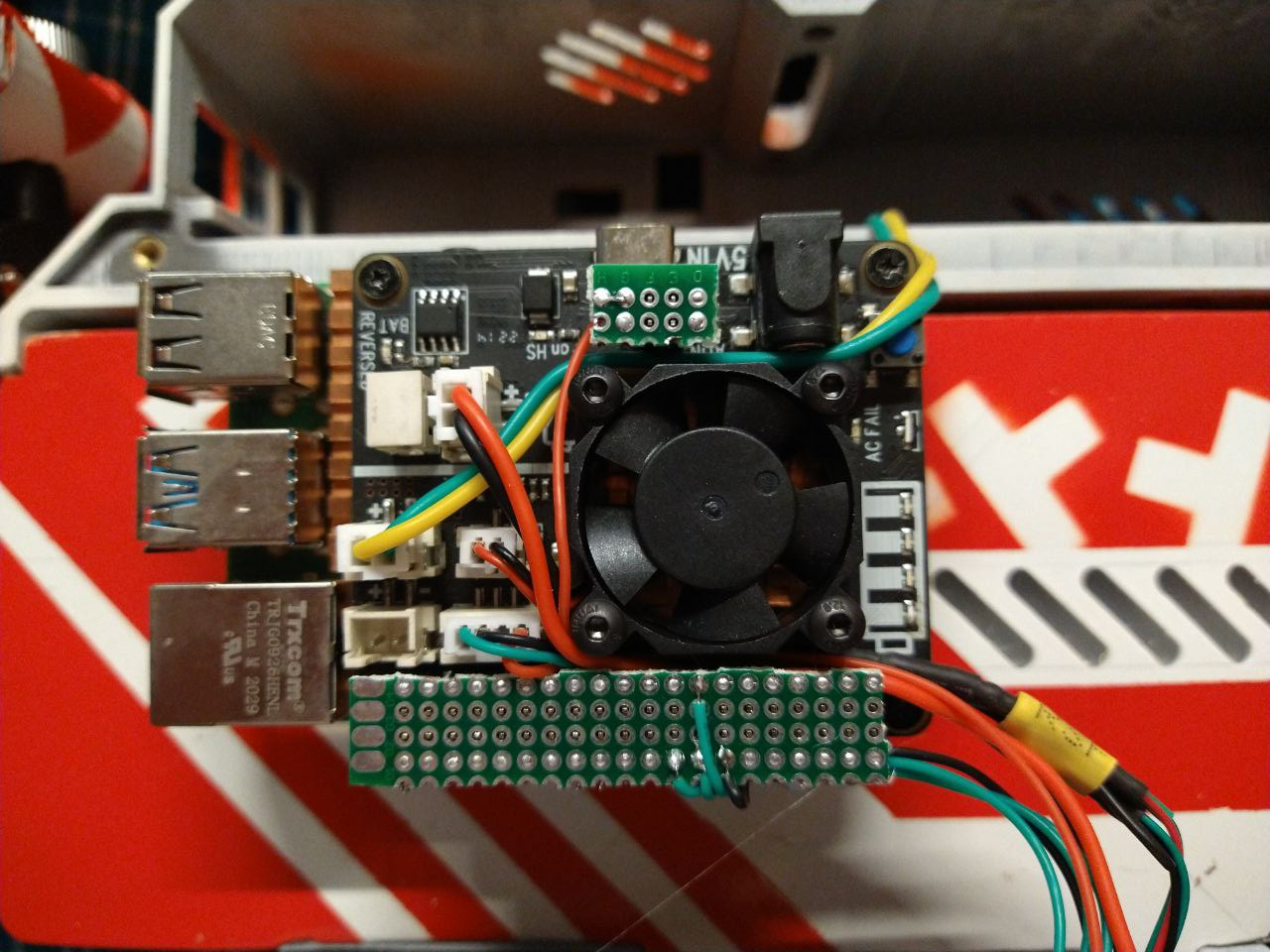
The board also comes with separate indication trigger pin alongside of power to user leds - this will allow to trigger charge level indication with whatever signals you wish, basically (as long as it is within 3-5V range). I will use VIN pin on UPS hat so that when charger is connected - indication panel will display current charging level. Remember though that this battery level indicator only relies on direct battery voltage measurement - hardly a precise way of telling if tanks are full.
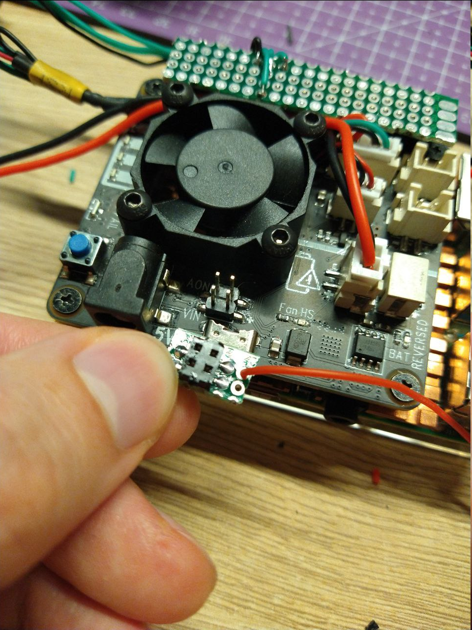
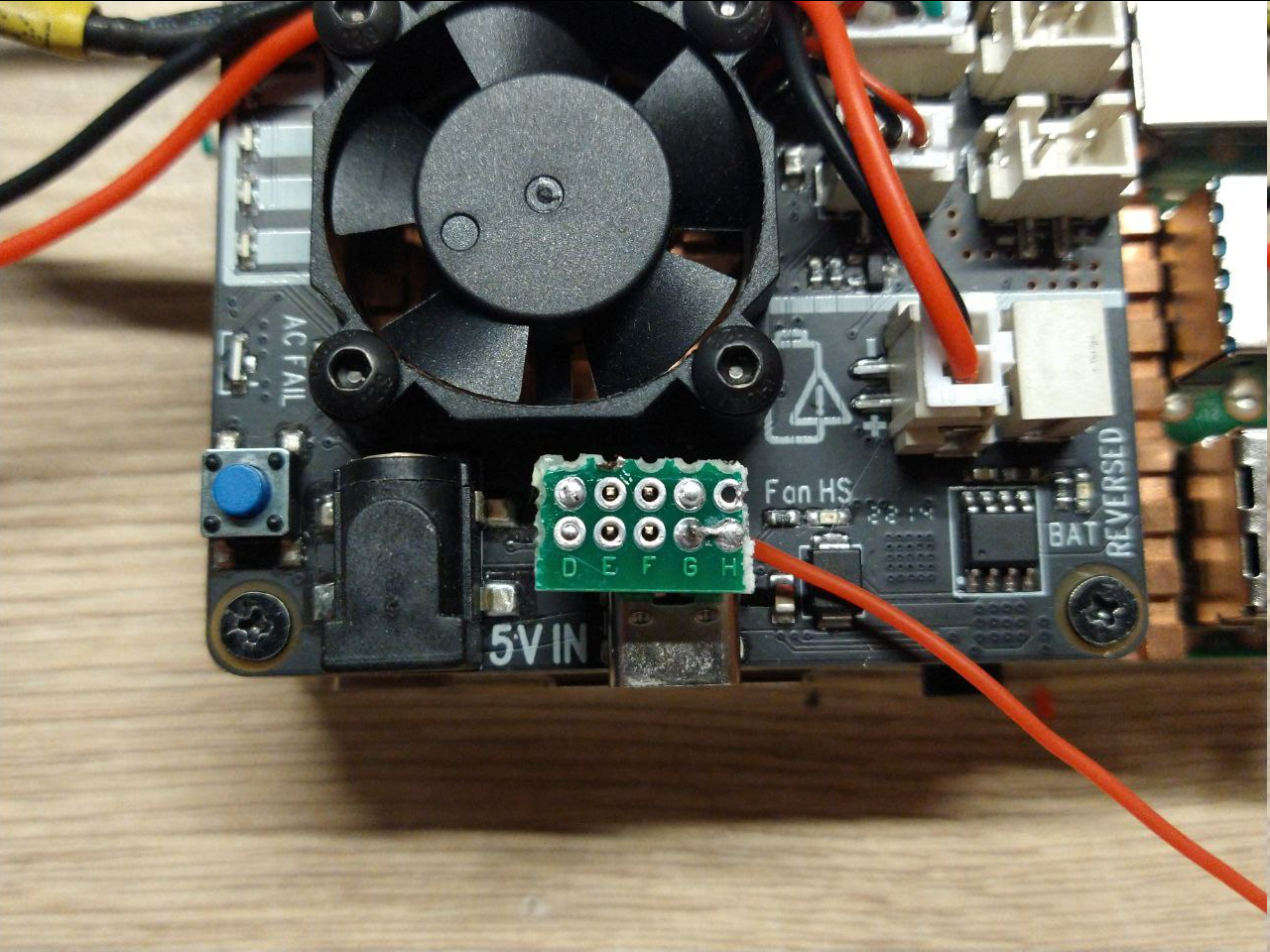
Grab another low profile 2.54 header - there is not much space around motherboard to fit full size ones. Solder it to a piece of smallest perfboard you could find, bodge a jumper wire to "VIN +" near USB power connector on UPS hat and route this wire to CHRG pin on USER connector on the indication board. Since this pin active high, you can probably also add two diodes and connect Pi GPIO in parallel, so that you also can control indication from the Pi, but i'm not going to do that for now.
 One nice thing about this little connector board is that it clamps display power connector under it so it won't fly around when you are working with the board.
The amount of parasitic additions asks for another HAT to be designed.
 There ain't much new to demonstrate though, i've shown how indication panel works before but here is a more marketing friendly action which shows how new leds flash and how board reacts to charger connected.
On less important note, i've found these cool angle USB connectors connectors to tidy up the left side of things

 And free advice for the most patient readers: please have enough sleep especially when actively working on a project. Assembling the board was not really hard, however when parts arrived, it's either me or the seller who swapped N-mosfet reel with P-mosfet reel, which took me 2 hours at 3am to figure out after the fact that i've soldered both onto the board (basically means that both of them are open when power is applied, which was not the intended effect).
But the most clear demonstration of what sleep deprivation can do to your ability to build blinky things is the realization that i've soldered Q2 gate transistors... 90 degrees rotated from how they are supposed to be fitted. Which made Q2 always open even when i figured out which was the correct reel the seller sent me and it drove me nuts.
And before a keen eye says "your PCB design allows to do that" - that PCB was also designed mostly at 2-4am in the morning, so, yeah, sure.
But hey - the relief of fixing your own mistakes is worth it, right?

Discussions
Become a Hackaday.io Member
Create an account to leave a comment. Already have an account? Log In.