 Chris
ChrisThis is going to be somewhat of a retrospective. Over the past year I have been working full time and have been concurrently completing my graduate degree as a full time student . It's been a lot of work so if things get a bit disjointed in the narrative that may have something to do with it. I've got like, two brain cells, so this has not been an easy project!
The intro may not have made it clear but this was supposed to be a weekend project for a quick, all purpose, dev board of my own. I was shooting for a half step above breakout board for the RP2040. With that in mind a primary goal was to break out ALL the pins. On the stock Raspberry Pi Pico you only get access to 26/30 GPIO pins. I'm paying for 30 pins of GPIO so gosh darn it I want to use all 30 pins if I feel like it! That's of joke of course, I'd be sick of layout too after spending who knows how long laying out custom silicon.
But then my cheap brain cell gets all worked up with this lofty pin-breakout-goal presented by the flexible brain cell. Why? Because more signals means more pins, which means more board area, which means more money! So the first question was: how small can I make the make the board. The second question was: how could I break out all the signals in a reasonable way?
The answer to the first question was clear: I'd make it 1 square inch. Why? Well that's the size of the RP2040 Stamp, which I'd argue isn't really a development board and more of a daughter board or maybe an SoC. Sure it's technically hand solderable but what's the point if you need a carrier board to even use it? Then it's no longer 1x1 inch!
Answering the second question was a bit more difficult. After many minutes of thinking my two brain cells presented me with:
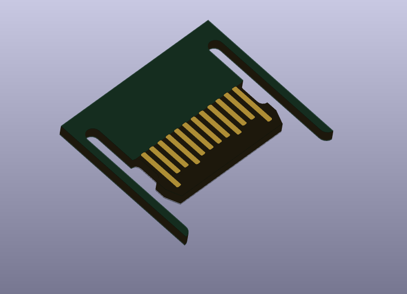
The Thad - A Through-Hole Pad.
Clever name, I know. Hopefully a clever solution too. It's literally just a square pad with sort of small plated through hole down the middle
Yep! That's all it is! But sometimes the simplest solutions are the best solutions. Obviously this gives you a nice place to solder jumpers, but more importantly, it also allows you to hand solder the board down another circuit board without having to deal with the 2mm pitch of the RP2040 Stamp. The hope is that if everything is tinned properly then the solder will follow the heat down the plated hole and be drawn onto the bottom pad through capillary action. I don't really know what capillary action is but it sounds applicable in this case.

Space those bad boys out on a 0.1 inch grid and stagger them with the regular header pins and it feels like just maybe we found a cool solution. There's one more cute little trick that I'll show in the next post that really takes this concept to the next level, so stay tuned.
Alright great! So we have the Thads taking care of breakout duty but man, my cheap brain cell wasn't quite satisfied. I mean sure, those pads don't technically cost money, but look at all the space they are taking up! We're only working with one square inch here, buddy! We better do some serious space saving somewhere else. And oh boy did we save some space in promote the most questionable way possible. Presenting:
Free USB-C Connector - USB-C, but SKINNY
If you think about it. What do you really need in a USB-C port? Obviously you'll need the metal contacts because electrons tend to flow better through metal. Or so I'm told. You'll also need something for the metal to sit on, so substrate material is pretty non-negotiable too. The rest? Well, do you really need it? "Strain relief something something," I hear you mumble; but do you really need it. You may say yes, but I say no!
Hear me out. For something like a phone or a laptop, of course this would be a horrible idea. You would snap this little piece of fiberglass off in an instant as soon as you forget your phone is plugged and try to roll over while reading Hackaday in bed. Ports for consumer applications like that need to survive potentially thousands of mating cycles and all sorts of wear and tear. The port on a microcontroller? Not so much. If some how you manage to wear out the connector on a CRAPi board, with a few hundred mating cycles, congrats I guess! Thankfully for the more enthusiastic USB users, the CRAPi2040 breaks out the USB lines of the RP2040 to 0.1 inch header.
With our trimmed down USB-C connector, we save precious board real estate and frustration with the soldering iron. Interestingly, I haven't really seen this done before. There is this project from a few years ago using Eagle (RIP) that attempts to create a PCB USB-C connector but there was never a report of success. So I certainly won't say that I am the first one to attempt this idea, but it seems like I might be the first one to attempt this idea on a development board.

You might say it's a bad idea, or a crazy idea, maybe even a crappy idea. Thankfully, I am willing to push the boundaries of crappy ideas so that you don't have to. So I spent some time studying Section 3.2 of the "Universal Serial Bus Type-C Cable and Connector Specifications," also so that you don't have to. The result? The beautiful KiCAD footprint that you see below, which is designed to be integrated into the Edge Cuts layer of the board outline. I think it looks pretty slick.

Ready for the answer? Wanna look again? It's 0.7mm. You would know that if you read the spec!
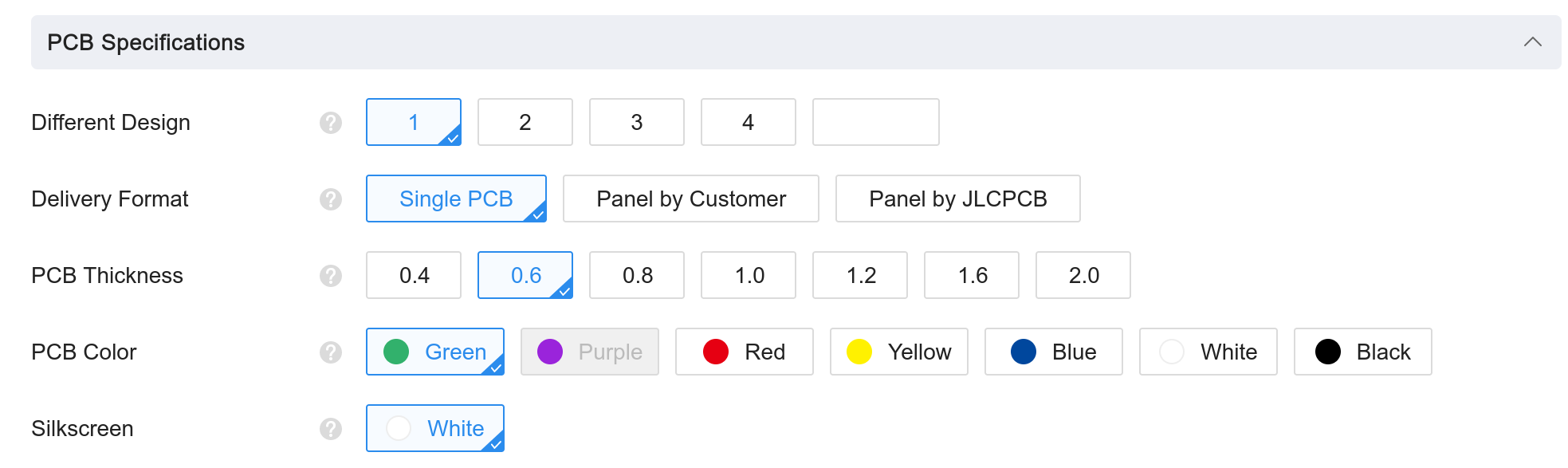 Thankfully, JLCPCB (because who else would I be using for this project?) gives the option for a 0.6mm board with some limitations on layer counter and silkscreen color. The color is for sure a bummer, but considering the journey that I was about to embark on I really wish I had the option for a 4 layer board. With ideas this crappy, sometimes the only option is to just push through with spit, grit and a whole lot of time routing traces in KiCAD. (spoiler: the connector it worked. If you have read this far then you deserve to know!).
While I thought the cheap and flexible brain cells had finally settled down, I was wrong. They both wanted one last tribute. Sure, fine, I can do that! I promise that it will be a border line crappy idea that might just be good enough to be useful. Remember, the name of the game is to add "free" features through PCB design. How can we make the board as useful as possible without making it more expensive? That's where the third crappy idea comes in: the Protogrid!

There is some logic to the pad spacing and functions too. I found that a 20 mil grid should be the most useful as a lot of surface mount chips have leads that are separated close enough to a multiple of 20 that you can get clean connections. Pins 1 - 8 are connected to GPIO. Pin 9 is VIN (5V), Pin 10 is 3.3V, and Pin 11 is GND. The vertical pads running down the middle are spaced in such a way that if you want to solder on a new USB port you can do so as most of them of 20 mil pitch on their surface mount leads. See? Options!
Miscellaneous Features and Rambling
The three major points listed above are really just part of the picture for this first revision. On the second revision you'll see that I pushed the boundaries even further. For this board spin though you'll see a few other cool features:
- RGB LED because it turned out to be the cheapest LED overall on Digikey?
- Lettering in solder mask instead of silkscreen for better resolution at smaller sizes
- Power enable and disable jumper just for giggles
- A single 2mm mounting hole
- 0402 Components (not cool, just bragging).
- A boot AND a reset button so you don't have to keep power cycling!
The (virtual) reveal.
If you read this far you deserve yet another reward (you didn't just scroll to the bottom, did you?). Below you can see a virtual picture of the completed board. All of the supporting components to the RP2040 were chosen to be as small and/or as cheap as possible.

 The eagle-eyed among you may have noticed that there is a discrepancy in the Protogrid between the KiCAD footprint picture and this render. That's my bad! Remember, this is a retrospective and my documentation skills aren't exactly on par. I forgot to take a better pictures of this first revision so the best I could do was the renders from my JLCPCB order.
 Lucky for you, because this is a retrospective that means you don't have to wait very long for the next post to show you how Rev. 1 of the boards turned out. As you can probably guess... there were some major issues....
That's all for now, stay tuned!
- (C)hris
Discussions
Become a Hackaday.io Member
Create an account to leave a comment. Already have an account? Log In.