 Chris
ChrisAlright here we go! In case you missed the last log, here it is! Check it out because what you're about to see will make a lot more sense. Just like the last log, this log is going to be a retrospective, but I promise that the next CRAPi2040 log to grace your retinas will be firmly rooted in the present!
We left off with the very first "completed" revision of the CRAPi2040 board. All told it probably took a few tens of hours to design and layout. Some of that time included picking out parts, learning KiCAD, and looking up reference material. But I would say that 75% of that time was for sure spent routing and rerouting traces and trying to keep my ground plane in tact. I'm going to be honest, the amount of time I spent laboring over that routing was probably not healthy considering I was supposed to be taking a break from school and only focusing on work and my friends and family.
But who cares about all that stuff. You're here to see that gorgeous board! So here it is!


Beautiful I know, even if my phone camera washed it out a little. You can get a really good look at the routing thought which I think is awesome. You'll notice that I didn't do a great job at keeping my traces on the top of the board so some current paths are probably longer than they need to but on a board that is only 1 square inch probably not a huge deal. To be honest, it looks a little crappy to me but hey sometimes you've just got to send it. The gerber files that is, to JLCPCB.
If those pictures don't satisfy you, say no more. I am lucky enough to be the proud owner of a garbage bin microscope! It's sort of hard to take good pictures with my phone through a microscope but it's better than nothing. Plus it's a huge help when trying to deal 0402 components. My eye sight is pretty good but this really takes a lot of the guess work out soldering these leadless components. To the surprise of no one, it's hardly smooth sailing from here so I'll take every advantage that I can get.

At a first glance under the microscope things look GREAT. I didn't really know what to expect from JLCPCB because these boards were literally 20 cents each. The driving factor for such a low cost board, as you may have noticed, is that I went with a HASL finish on the copper pads. This was my first time even hearing about the process so I needed to look into it.
HASL stands for Hot Air Solder Leveling and the process basically involves dipping the entire circuit board into a vat of molten solder to tin the exposed copper. As the board is withdrawn all the excess solder is blown away by hot air knives. Or so I am told by Google. Looking at picture definitely helped.

This is opposed to the typical ENIG (Electroless Nickel Immersion Gold) process that most "normal" PCBs are put through. This is the one that gives you those nice shiny gold pads. The ENIG process deposits a layer of nickel and then a layer of gold on to all the exposed copper, without using an electric current. Nickel is essential for preventing the gold from diffusing into the copper and of course the gold is great to solder to and provides corrosion resistance. But obvisouly the most important part is that ENIG is prettyyyy.
 The (G) stands for (G)old so it's cleare why ENIG would cost more money than HASL. When I sent the boards away I already knew that I was going to need to do another board revision so I didn't bother getting the good stuff. That turned out to be a great choice considering all the issues these boards would have. I'm not surprised, just disappointed.
They Thicc.
As a reminder, the PCBs need to be around 0.7 mm for this crappy USB-C connector idea to work. The closest option available was 0.6 mm from JLCPCB so it wasn't even a given that these boards would work. Unfortunately, we would not get to see if that 0.1 mm really made a difference because the PCBs that were sent were 1.6 mm!
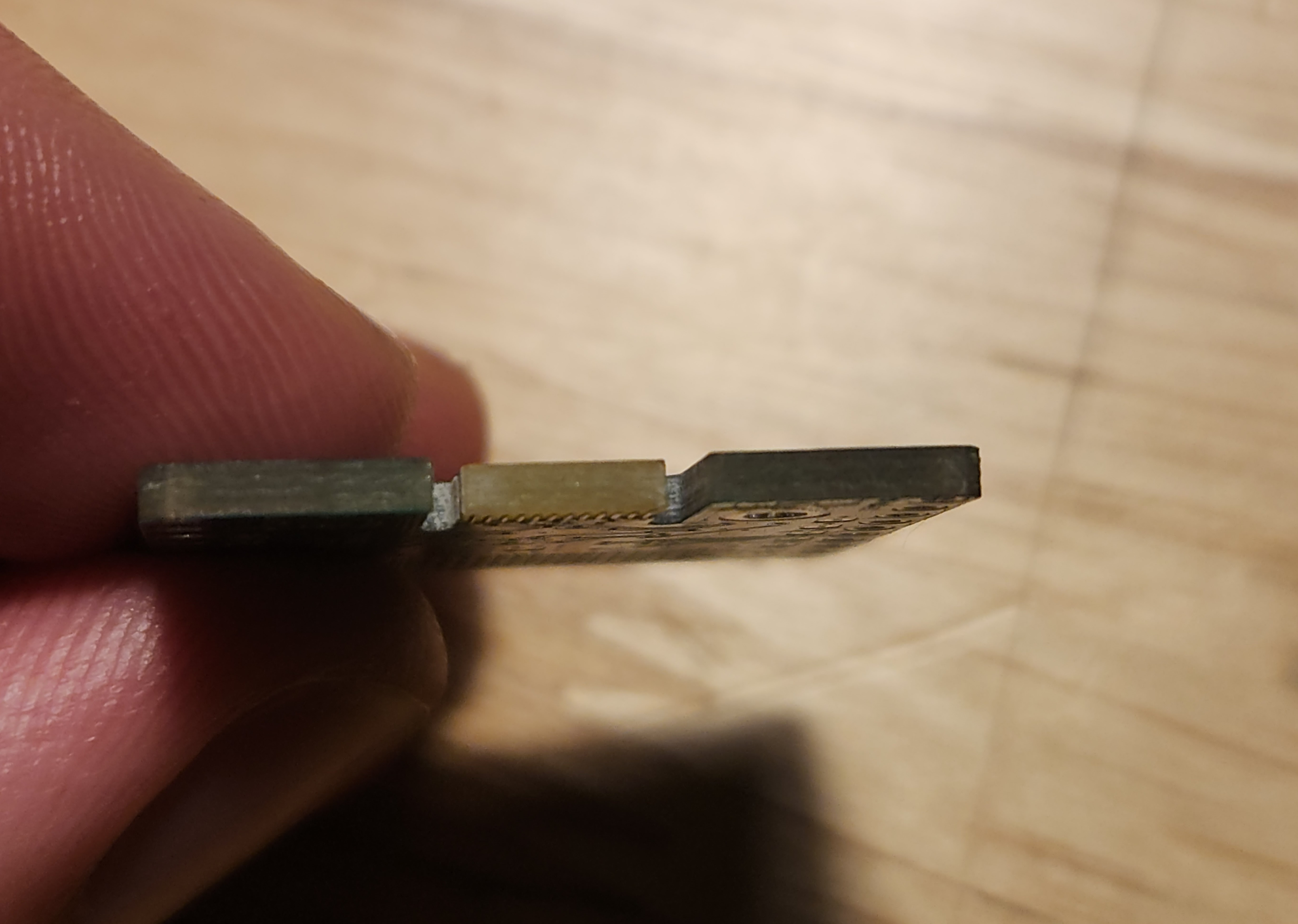
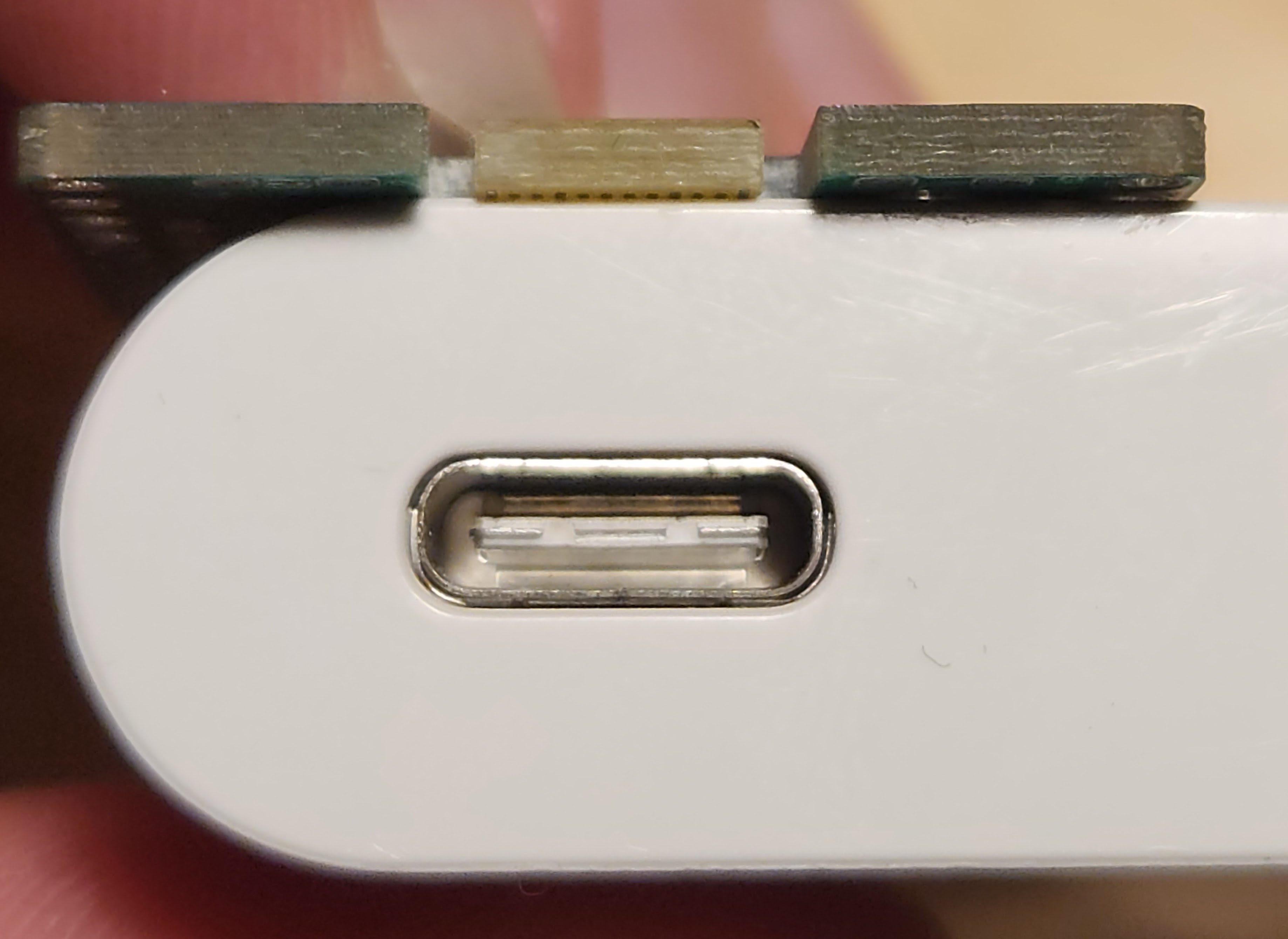
It's pretty easy to tell that is way thicker than we wanted but just to really send the point home here is a comparison picture of a "tongue" that is the correct thickness.
So I was super bummed about that. I thought that for they had made some sort of mistake in my order. I mean this idea was the whole basis for this project in the first place! Surely I couldn't have made the mistake! Yeah well, a quick visit to the JLCPCB invoice showed that I did actaully order 1.6mm by mistake. When I was ordering these boards it was probably about 3 a.m. and I had reuploaded a few times. I thought I was careful to select the thickness but I guess the lack of sleep got the better of me.
Lesson Learned: Don't order PCBs after midnight.
Through manly tears and gritted teeth I told myself I could still make the most of it. Thankfully I had broken out the USB D+ and USB D- lines on the RP2040 so that I could still program the board with a chopped up USB cable. Plus, there were still plenty of other things to check out!
Solder Mask not Silk Screen
One of the things that I was most interested to look at was the resolution of the text in solder mask versus in silk screen. I had a feeling that the JLC silkscreen would not be fantastic considering the price. I'm workign with a pretty limited amount of board real estate and so I knew that the pin lables would end up being pretty tiny. I also had a feeling that the resolution of the solder mask would be far better than the silk screen. I turned out to be right!
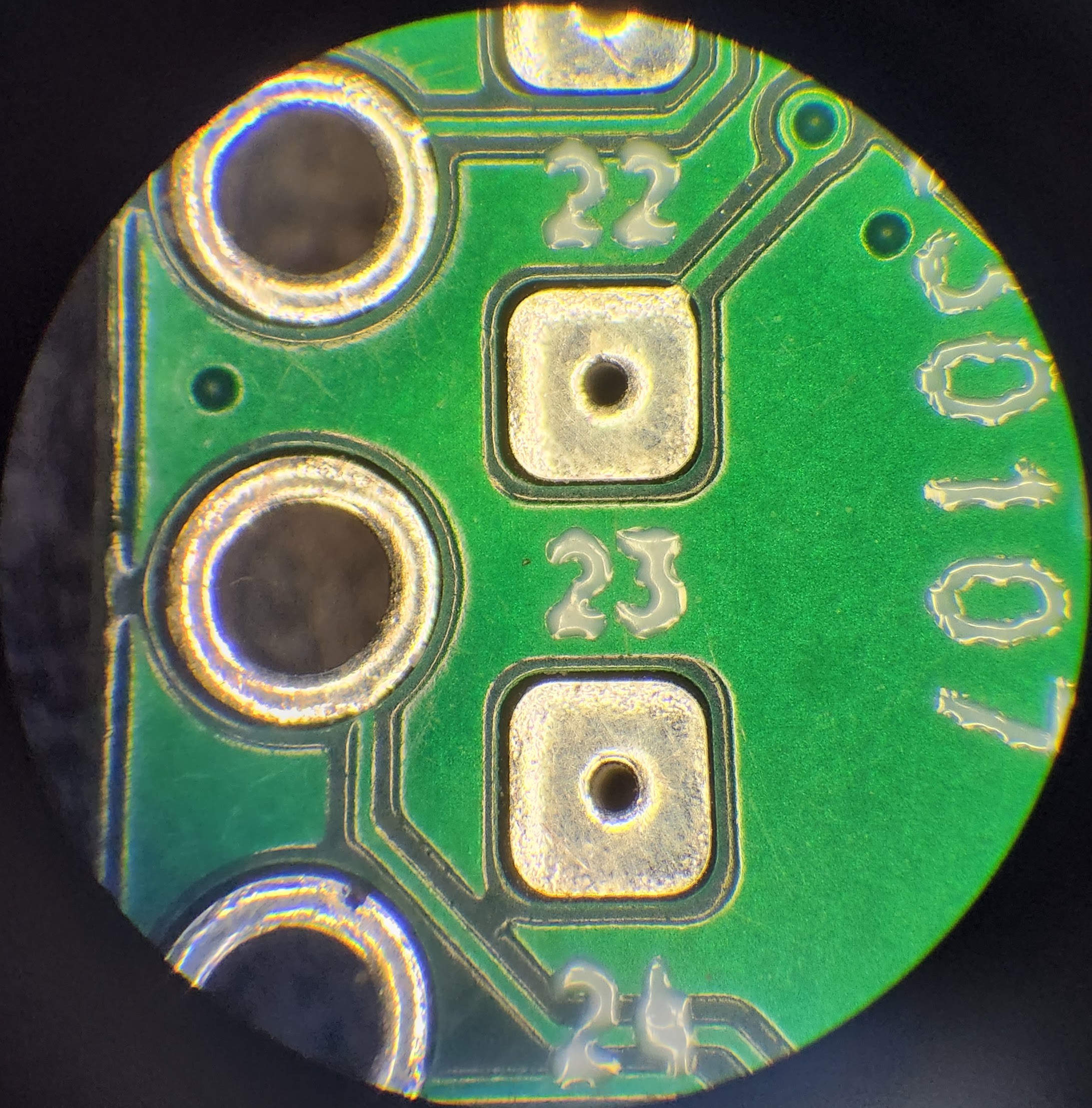
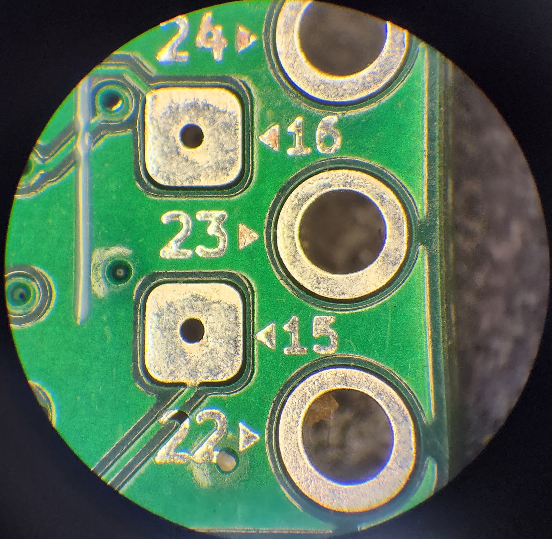
I was surprised to see how just how chunky the silkscreen looks under the microscope. Granted, this isn't particularly high quality silkscreen, but still. The name of the game here is cheap, remember? It's just a reminder that you get what you pay for. The solder mask text looks far far better. The text size of the "23" is 1 mm if I remember correctly and the size of the "15" is 0.75 mm. But if we turn off our microscope the story is a bit different .
Taking a look again at the phone picture, you'll noticed that the numbers aren't super readable. That's not just a result of the crappy picture. In real life, the numbers are actually pretty hard to see. This is because the HASL process that we talked about earlier leaves a nice shiny silver coat of solder on all the exposed copper of that board. Tiny silver letters don't show up well with a green background. If I had gone with the more expensive ENIG process I am sure that the letters would be been much more legible. Ironic.. You can see that the BOOT and RST text worked a bit better because they are bigger, but still not ideal. The BOOT and RST text also highlight another issue with putting text in the solder mask: you need to sacrifice a lot of ground plane. I got lazy towards the end so I wanted to see what vias would look like when placed in the solder mask text.
Evidently you can push text-in-solder-mask pretty far! But text this small quickly becomes useless to the naked eye. I guess you can leave secret messages for microscope owners though!
Lesson Learned: Under certain conditions, putting text in solder mask can be a good way to get around silk screen issues.
For this board though, it didn't really work out. With the next revision, it was clear that I was going to need as much space for traces as possible. I couldn't really afford to waste space with labling. Although, under the right conditions I'd love to try this trick with an ENIG board, so I will keep this trick in my back pocket.
Looking at the ProtoGrid and Thads
I'd say that both the ProtoGrid and Thads turned out pretty well too! You can see that the GPIO labels for the ProtoGrid connections are visible under the microscope but almost invisible to the naked eye which is a bummer. I did incorporate a nice little trick for keeping tiny pads stuck down though, and that's to drop a via in them. You won't be able to (and shouldn't!) do this for most l pads but in this case it made sense and made a big difference in pad durability. I didn't show it here but even after some casual testing the pads without vias on the grid came up very very easily. So it's pretty clear that in later revisions I would need to try to make them a bit bigger so they don't just flake off under a soldering iron. I was feeling a bit discouraged at this point so I didn't really test the Thads but I'm still convinced that they will work and will test then in Rev. 2!
TIME FOR ASSEMBLY
Alright, that is enough inspection. Let's put the thing together and see if it actually works! This post is already getting pretty long so I am going to kind of cruise through some of this stuff.
First question is: to solder paste or not to solder paste? With all of these 0402s and non-leaded components I chose to solder paste, at least initially. I also got myself one of these.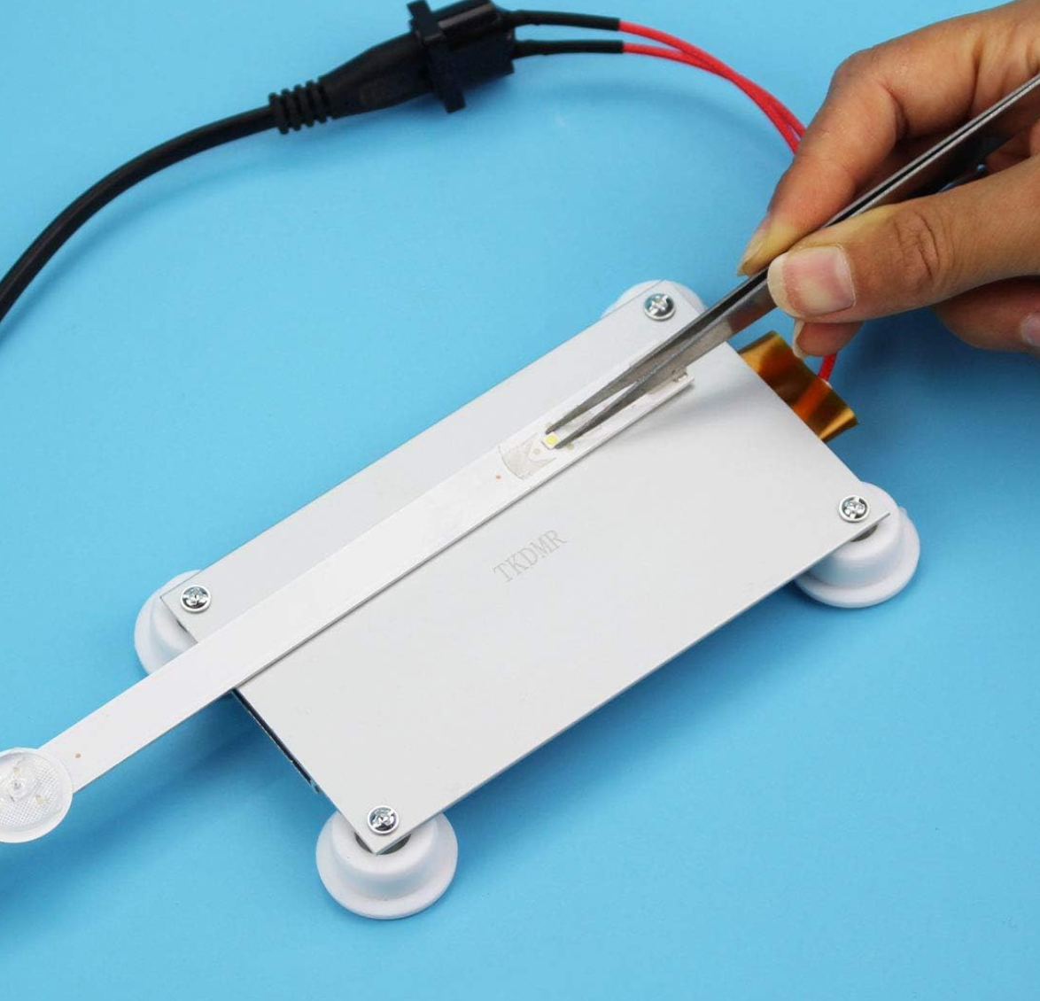


It's a positive temperature coefficient (PTC) hotplate that heats up to +300C (in other words hot enough) as soon as you plug it into the wall. The nature of the PTC heater inside the piece of extrude alumnium means that it regulates it's own power output. For the circuit building snob this is no replacement for a proper oven or hot plate that can execute carefully controlled reflow profiles. For me though, falls firmly into the "crappy but useful" territory I have come to know and love. Plus the thing only costs like 15 bucks, so it's really hard to complain. It melts my solder and that's all I can really ask for.
This did come back to bite me a bit though, more in the Rev. 2 post about that.
Turns out, the stencil that provided by JLCPCB wasn't really suitable for this fine of work. It was too thick which meant that too much solder paste would be applied to the pads of the PCB. I was able to mitigate this somewhat but placing the populated PCB on the plate and then plugging it in so that it more gradually got up to temperature.
Ultimatly though, the HASL turned out to be a good move. With so many solder bridges I gave up on the paste and just stuck components to their pads with lots of flux. The little bit of solder on the pads from the HASL process was enough to form good connections with most of the components. I could then go through with a little bit of paste more selectively, and fill in any missing connections via soldering iron and microscope.
Lesson Learned: Paste is not always the answer for SMDs!
With the construction method sorted, I finally started getting some parts on to the boards!
Linear Regulator Woahs
It's worth noting that I did take somewhat of a systematic approach when first assembling the board. The first chip that I needed to prove out was the linear regulator that drops the 5V to 3.3V. I choose the MIC5528-3.3YMT-TR because this thing is TINY. The datasheet says 1.6 mm by 1.6 mm. The datasheet also says that it can push out 500 mA, assuming you don't mind a crazy high junction temperature and almost immediate thermal shutdown.. Realistically, 100 mA of continous output is more reasonable to expect from this chip but it's nice to know that it won't brown out if there is a current spike.

Yep, those are the tips of tweezers right ther. This thing is small and I wanted to make sure tot do a REALLY good job NOT shorting out pads when I was reflowing. For some reason though, they kept getting burning hot when they were hooked up. I was convinced that I was shorting the pins or that I had gotten the footprint wrong because every single LDO suffered the same fate. Well turns out my reflowing was totally fine.

 Once again I experinced that feeling of trying to be too clever for my own good. The "+" is created by a lack of solder mask on the ground plane. I thought I was so clever with this nice little plus sign (see above). The pad directly next to it, the one whose function it is describing, is of course the 3.3V RAIL. I had solderd jumpers on to the 3.3V pad to make sure I wasn't trying to probe through oxidation or flux. I had inadvertently bridged that < 1 mm gap with solder and didn't even notice... making a dead short between ground and 3.3V. It's funny how the steps that I took to be careful with my measurements ended up making my life harder.
Lessons Learned: Don't be too clever for your own good. and honestly so many more.
Mo' Flash Mo' Problems
Feeling pretty silly about myself, but getting a nice 3.3V from my LDO all the same, I pushed on. With the power sorted I moved on to the clock crystal, LED, and RP2040. Making sure to savor each little victory. We got a clock signal on the 'scope, a glowing red LED, and most importantly: A RP2040 MOUTNING AS MASS STORAGE!!!!! LET'S GOOOOOO!
With my spirts flying high I dragged and dropped a blink.u2f file on to the Pi and after a second the drive disappeared. OUTSTANDING. I'm on top of the world right now thinking about how awesome it will be to have my very own dev board and then disaster!!!!
Only a few seconds after dragging and dropping that file the RP2040 REAPPERARED???
That's pretty odd, surely that must mean it's a flash issue. I had this same behavior when I tried to power on without the flash chip installed. I figured that I had probably had just bridged a pad on the flash chip. A few reflow attempts later and no dice. The RP2040 was inscently presenting itself to the computer.
Just to be sure that I had all my connections right I under took the dead bugging of my lifetime. Thank goodness for the microscope and that I didn't drink any coffee that day. And by the way, that's not enamaled magnet wire. Those are individual strands of copper wire that I pulled out of a bread board jumper cable. Yeah this was not a fun day.

With my flash deadbugged, and my board crusty and dusty but outputting 3.3V and a clock signal I was ready to make that LED flash and for the RP2040 to stop resetting itself and........... NOPE. Even with the beautiful PCB that you see below it, was the exact same story. The RP2040 would mount as soon as I plugged it in, regardless if the BOOT button was held down, disappear briefly when I gave it a file to eat, but then come back a few second hungry for more.

At this point I was beyond frustrated. The symptoms seemed to indicate that the flash was not being detected for some reason. Now that I was 100% that everything was connected correctly in the real world, that must mean there was a problem on a virtual world of design. Surely I couldn't have made a mistake in the schematic, right? I mean the flash connection is so straight forward! Yet again, to no one's surprise. I was wrong.
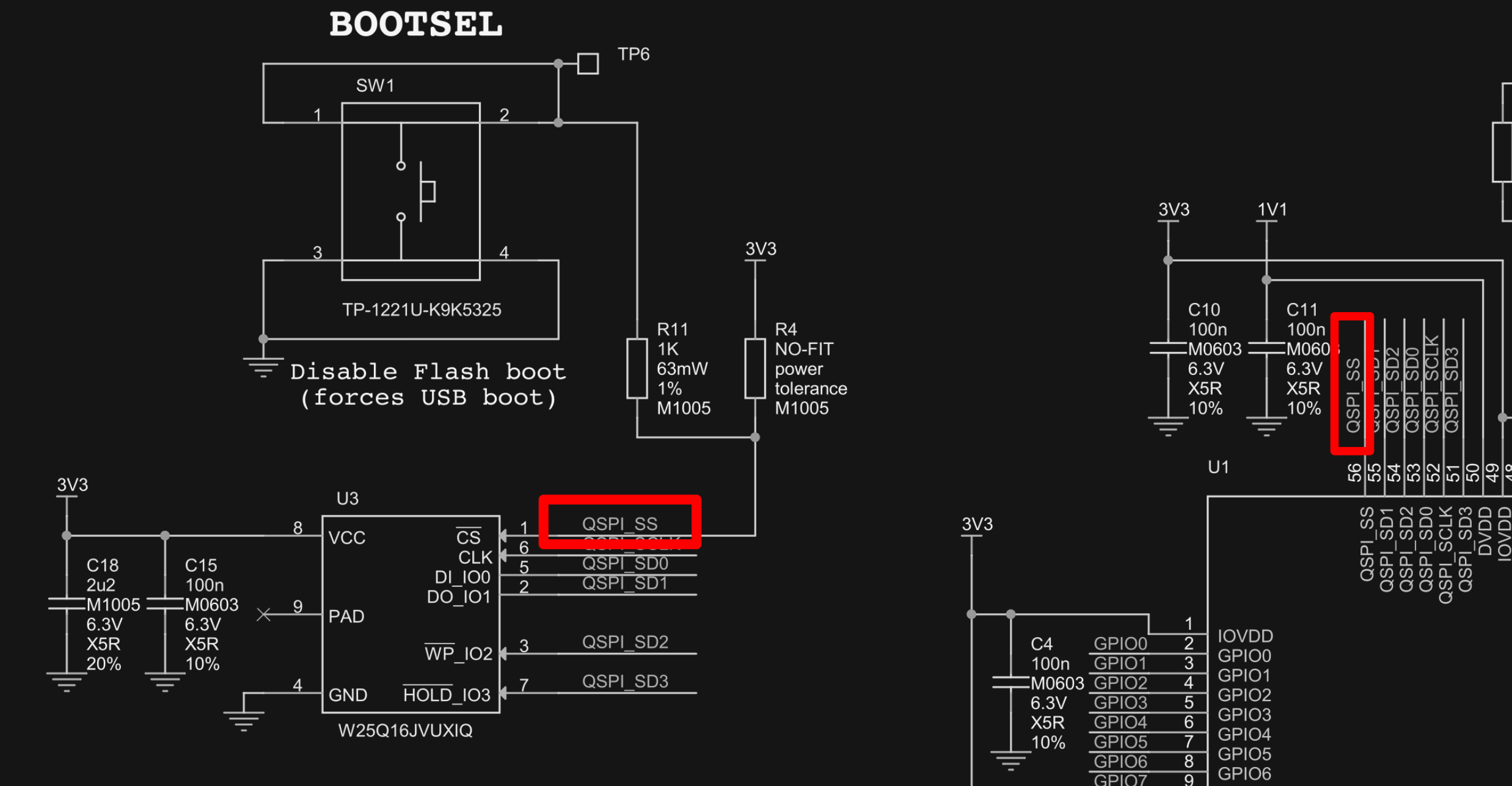
Taking a look at the schematic from the Raspberry Pi Pico, you can see that the QSPI_SS signal is clearly connected to both the button and the RP2040. I had missed that connection on my schematic. The flash chip was only connected to the button. So without the ability to strobe the CS pin on the flash, the RP2040 didn't detect that the flash was even connected, thus giving me the behavior I was seeing.
Lesson Learned: Never overlook "simple" connections
Once I had installed the approriate bodge wire the RP2040 no longer thrust itself at my computer's file system, which is the good news. The bad news? I was never really able to get a fully functioning board on the this revision. Getting the RP2040 to mount ended up being unreliable and I sort of got an LED to blink once or twice but it was nothing worth showing.
By this time grad school had started back up and my day job was burning me out too much to keep pushing with this revision of the board. Demoralized but not devestated, I was determined to make Rev. 2 a success! As soon as finals were done of course....
Sorry for the long post, and I wish that I could ended better for this revision. but fear not! In the next post we will see Rev. 2 and that ladies and gentleman is an outstanding success which will finally catch us up to real time.
If you made it this far. I am very proud of you, just remember the best is yet to come!
- (C)hris
Discussions
Become a Hackaday.io Member
Create an account to leave a comment. Already have an account? Log In.