 Chris
ChrisPreviously, we took a look at some gorgeous ENIG plating, clever silk screening, and a USB-C connector that consisted only of the 0.6mm PCB substrate that the rest of CRAPi board lives on. Honestly, I almost didn't even want to put the boards together. Seeing them come out so well made my week! The thing is, this isn't my first rodeo, I know how these things go.
Here I am feeling like a smarty pants with some shiny boards and cute little components, but I already know that this isn't going to work on the first try... but we must push on! The only way to turn the unknown unknowns into known unknowns, and eventually into known knowns is to just slap a board together and pretend that everything will work on the first try.
Now if I was smart, I would assemble the board bit by bit, ensuring that each component is soldered down and working as intended. If I was this hypothetically smart engineer, I would test my board by assembling things in the following order:
- Linear Regulator
Rule No. 0 of Electrical Engineering: Make sure it's plugged in. - Processor
Once the heart is beating, gotta make sure the brain is thinking - Flash
Once the brain is thinking gotta make sure the brain is remembering - Everything Else
Everything else is really just a bonus to me...
So with this plan in mind. I am going to completely ignore it and just put the board together all at once and hope for the best! Sometimes being smart and optimistic is mutually exclusive, and there's nothing you can do to stop me!
Assembly!
I mentioned it in the last post, but one of the changes between Rev. 1 and Rev. 2 was the move from 0402 components to 0201 components. In my head I knew that 0201 components were half the size of what I had gotten used to on Rev 1, but its a totally different thing to actually see how tiny these things are.
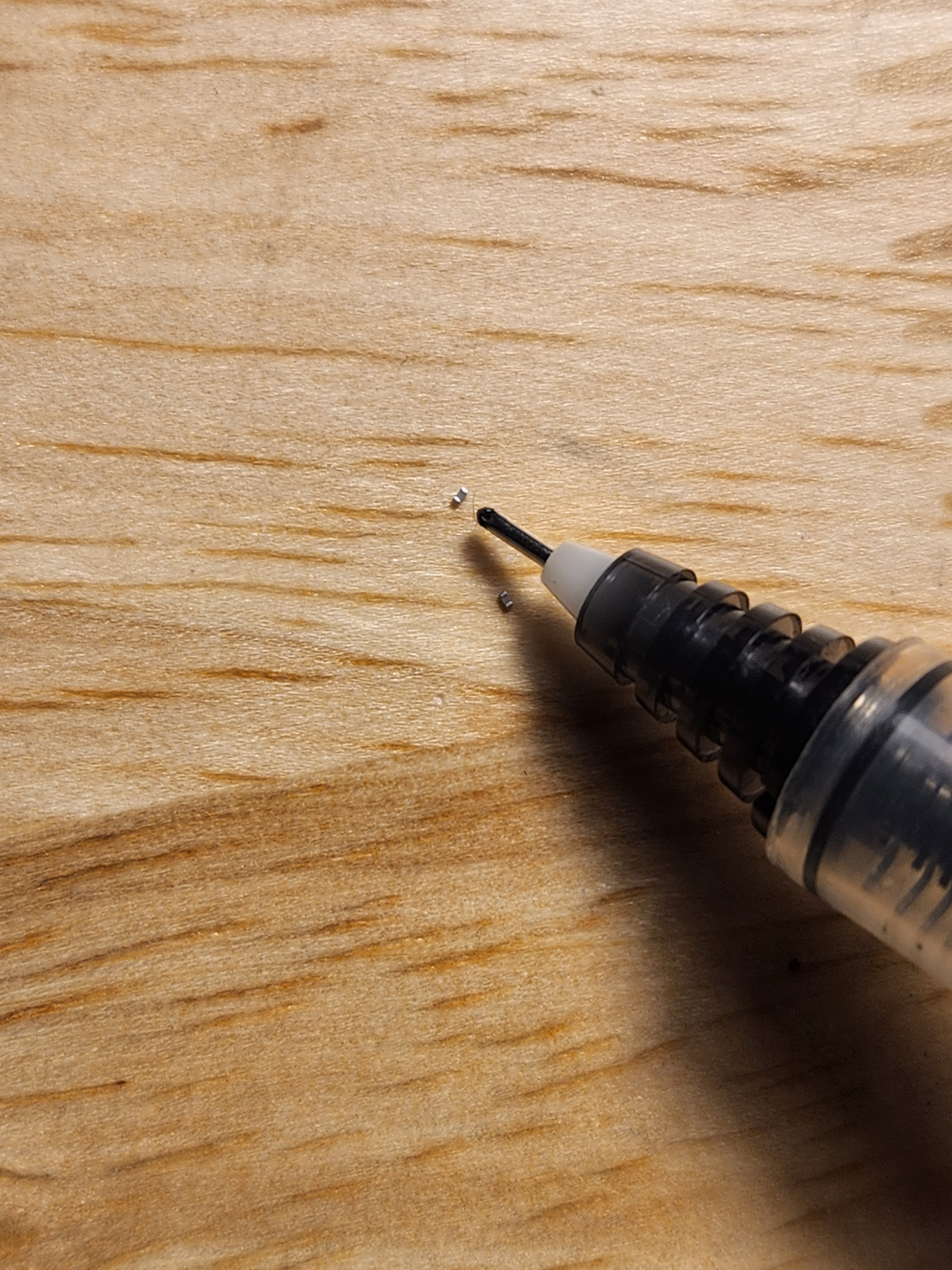
I mean look at this! Look how dumb and tiny they are! That's the tip of a pen! Man that was intimidating. I tried my best to only remove the number of components that I needed from the tape, but of course a few extras popped out now and again. It literally felt like brushing sand off my desk, if I felt it at all. At least clean up is easy. Just need to vacuum it up with the rest of the dust on my floor!
Once I got over the grains of sand that I would be trying to work with, it actually wasn't too hard. I had a pretty nice pair of tweezers and my eye sight is decent so populating and positioning those itty bitty Rs and Cs wasn't much harder than with 0402 components.
Armed with my solder stencil and paste, I lined everything up the best I could and gave it a good swipe to make sure that I got all the pads covered.
I carefully placed all the components into their respective locations yadda yadda, threw that thing on my crappy hot plate and watched the magic happen
Assembly Problem #1 - Solder Paste Trouble.
I mentioned that my cheap little hot plate gave me some problems in the last post and that I managed to mitigate them by heating up the hot plate with the PCB already placed on top. I did not have such luck with this new problem.
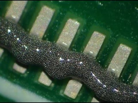
In case you have never seen it up close before, heres a random picture from the internet. Ypi can see that solder paste is just tiny balls of solder in a suspension of flux. Of course, the flux is supposed to melt first, and in the process clean the metal joint of oxidation that would prevent the solder from properly wicking on to the joint and mating the two surfaces
The interesting problem that I was experiencing is that the flux bubbling and boiling under my components created enough force to knock around the 0201 components. Because the flux melts before the solder does, there is nothing to hold those little grains of sand in place while the flux does its thing.
Eventually I'll look into the problem; obviously this has been solved.For now though, I don't really care!. Instead of mucking around with different types of solder paste or throwing down a few Alexander Hamiltons on a better hot plate I came up with a different method.
My SMD method in the form of an ordered list:
- Tin all the pads with my soldering iron. Tinning the tip of the iron and rubbing it on fluxed-up pads was good enough.
- Add more flux on top of the pinned pads - this is what will stick down the components
- Add your components to the pads (duh.)
- Throw the board onto the plate and and prepared to be satisfied.
There is something to be said about not over thinking....
You would think that this method would lead to the same flux bubbling issue, but it didn't. I guess the flux that comes out of my pen isn't as prone to the bubbling? Either way, it proves that you can do SMD reflow without making a mess with stencils and paste.
Assembly Problem #2 - Bendy Boards
Alright great, all the components stuck down soldered up, good to go. But then I noticed something: my boards were bending! After my first round of reflow I was looking at my pads under the microscope and noticed that a few of them weren't connected all that well.
I threw the board back on the hot plate to be reflowed and noticed the edges of the PCB starting to curl up! I am not sure if this was the sole reason for some of the missing connections. I am sure, however, that the crappy hotplate combined with the super thin PCBs didn't help. If I ever make these in quantity maybe I will splurge on something with reflow profiles. Better yet, I could use a CRAPi2040 board to modify a toaster oven and just make my own reflow oven!
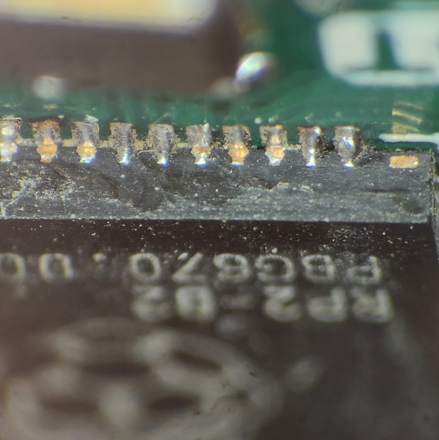
Here's an example of some poor connections on the solder pads. They aren't completely disconnected but they aren't great either. My (somewhat ironic) method of cleaning up these joins is just smearing a thin layer of solder paste on the side of the chip and hitting it with my soldering iron.
Still crusty, but better! I had to do this same process w/ the flash chip as well. Side note, does anyone know how to make things less crusty? I have seen some "no-clean" flux laying around at work and it seems to work as advertised. Having a microscope is a blessing and a curse...
TIME TO BLINK
Assembly was surprisingly smooth other than those two little snags. Once I got into a rhythm and warmed up a little bit, placing the components wasn't any worse than the 0402s from Rev. 1. It's funny how you pick up on little manipulation tricks when things are this tiny. I quickly honed the skills of kick-flipping components by gently pushing down on their edge. I also realize the importance of clean tweezers!!! Even just the tiniest bit of flux residue left on the tip of my tweezers was enough to prevent the components from releasing when they were dropped.
So after an intense learning period of about 45 minutes (roughly the time it took to put the very first board together) here is what I was left with!!!
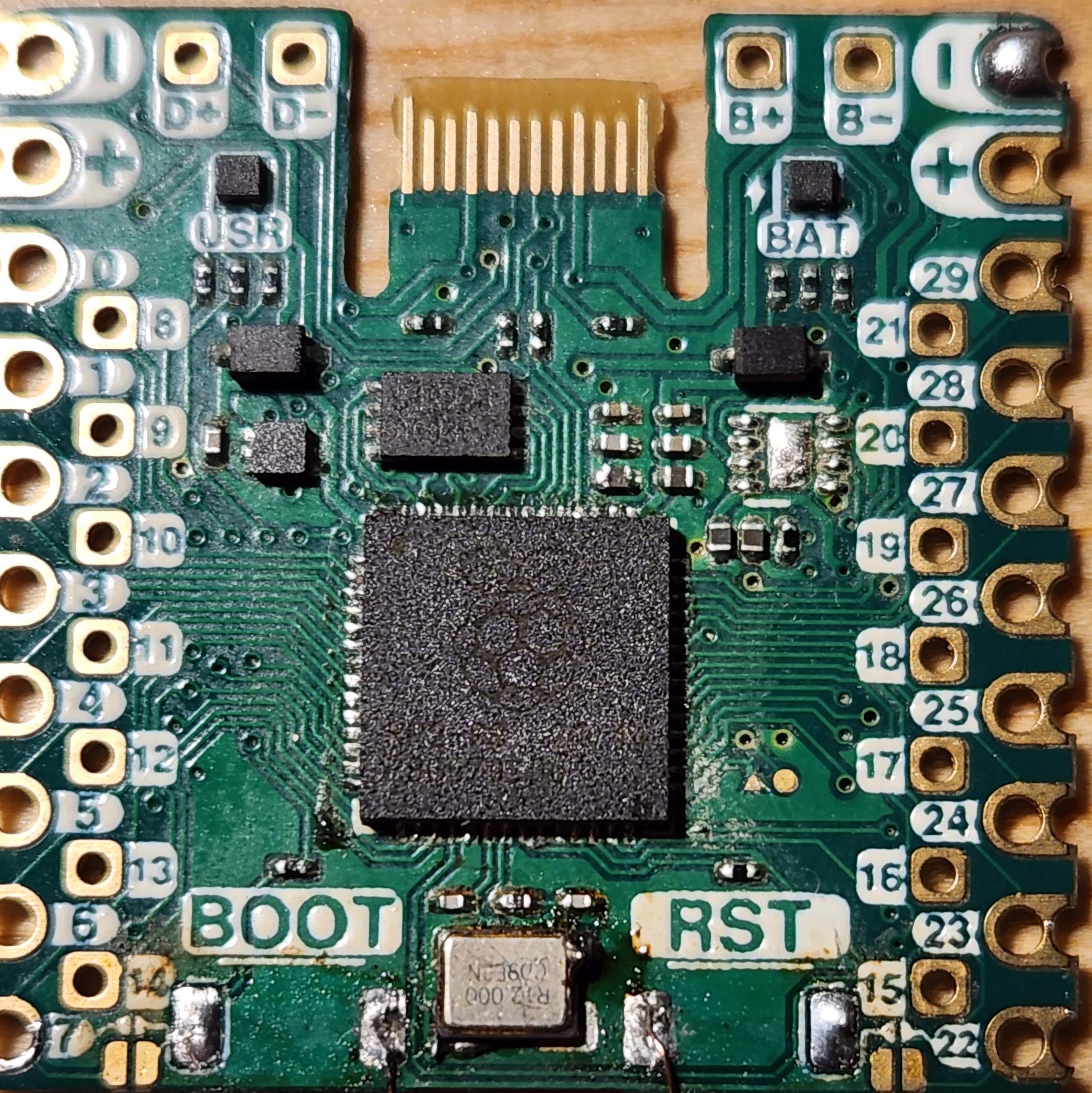
So pretty! (sorry for the shaky picture) Now time for the real question: DOES IT WORK???
Answer: NO!
When I plugged the USB-C connector in I didn't get any signs of life. The red power LED stayed disappointingly dark and there wasn't a peep from the RP2040 when I plugged it into the computer. Am I surprised? Nope! Disappointed? Maybe a little bit... Here is where things get interesting i.e. Why aren't things working?
The Troubleshooting Trifecta - ∆
Retelling this debugging process in chronological order would be sort of difficult because it took a few days and happened in a non-linear fashion. In retrospect, I may have addressed and solved problems that weren't the current cause of the non-functioning board but were still problems. The truth is I don't remember which problems were solved first. I've only got two brain cells, remember?
The problems:
- Matters of perspective.
- No ground for you!
- Missing capacitance on the linear regulator!
Problem #1- Matters of perspective.
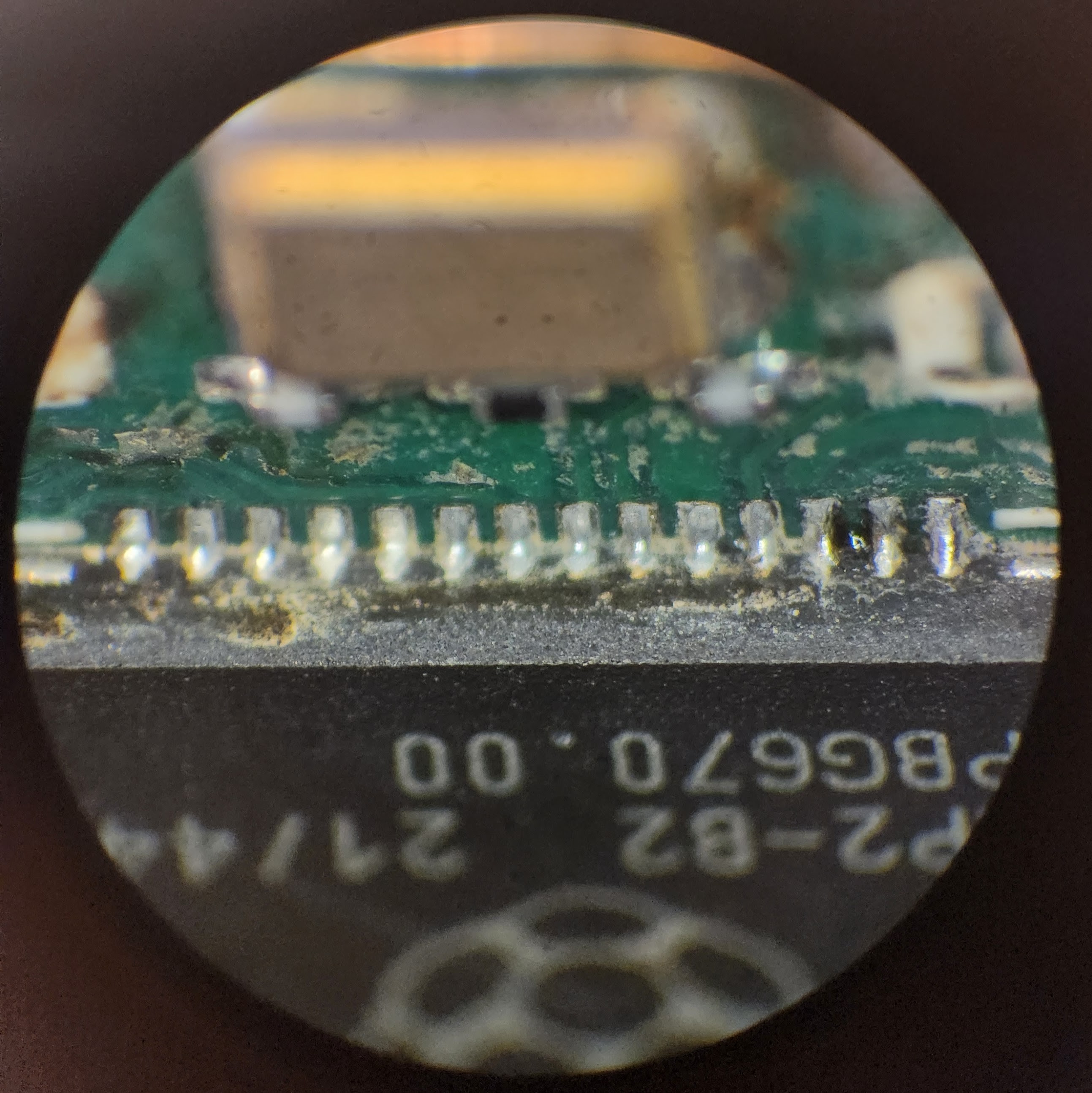
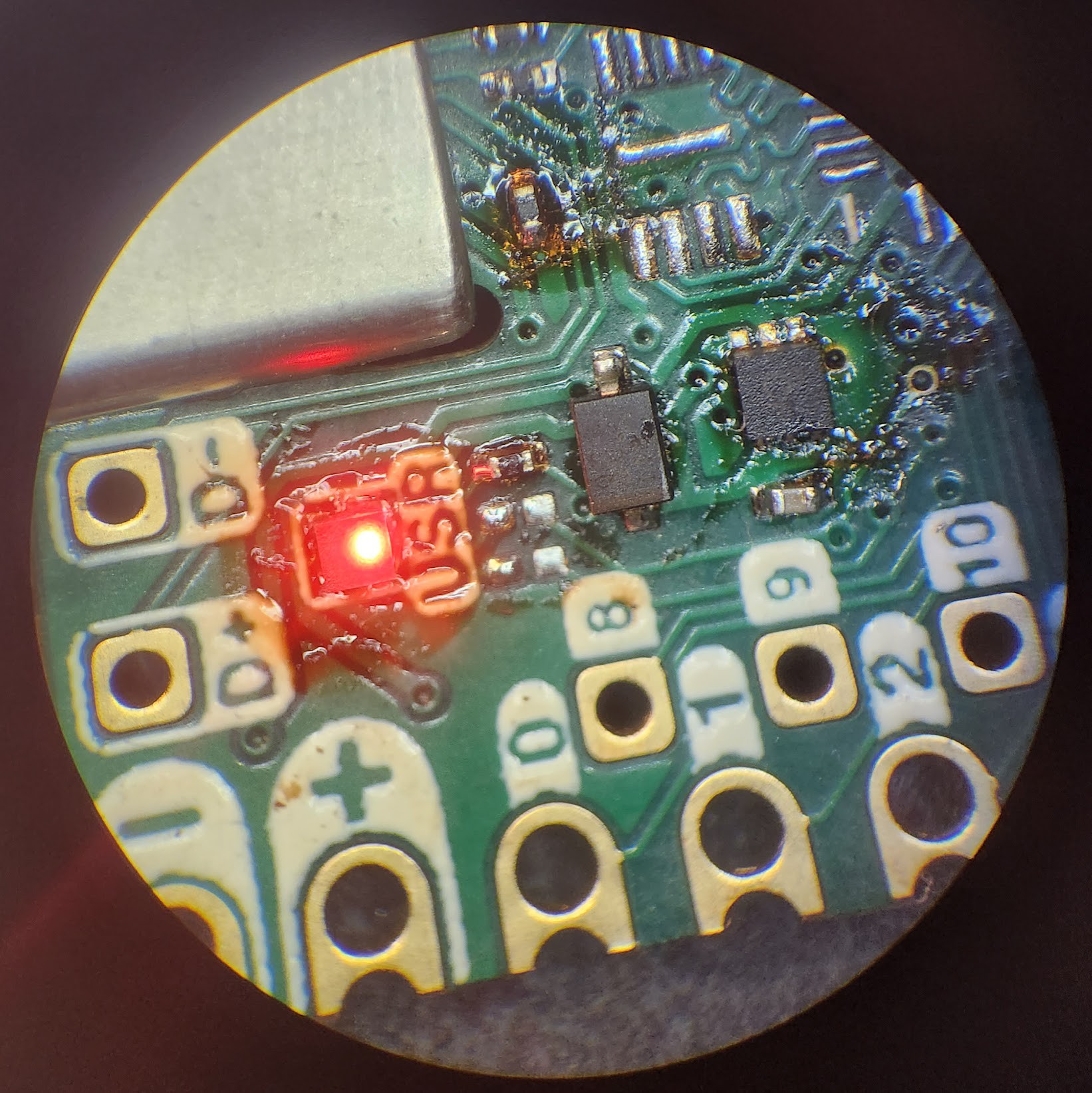
So the LED isn't lighting. Weird! Well first thing to check is if we are shorted to ground. A quick check with the multi-meter says otherwise! We are getting 3.3V out when plugged into a 5V USB supply. Nice! ...and surprising?? These linear regulators are TINY and I was almost certain that I had shorted something under the IC. Try to guess which chip it is in the picture above, I dare you! I was also certain that the LED wasn't either, so what gives?
Well: I got my silkscreen wrong!
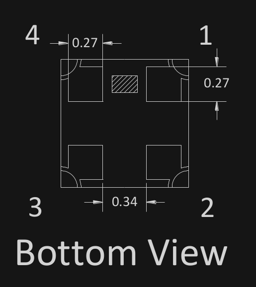
I am using a common anode RGB LED, that indicates polarity with a tiny little dot on the bottom. The data sheet gives the following diagram. Easy right? A bottom view of the chip and some dimensions, a few minutes later and I have my footprint in KiCAD
Here's that bottom view I was talking about.
And boom, heres the foot print. I even took some liberties with the pad design to hopefully discourage shorted pads. Notice any problems?
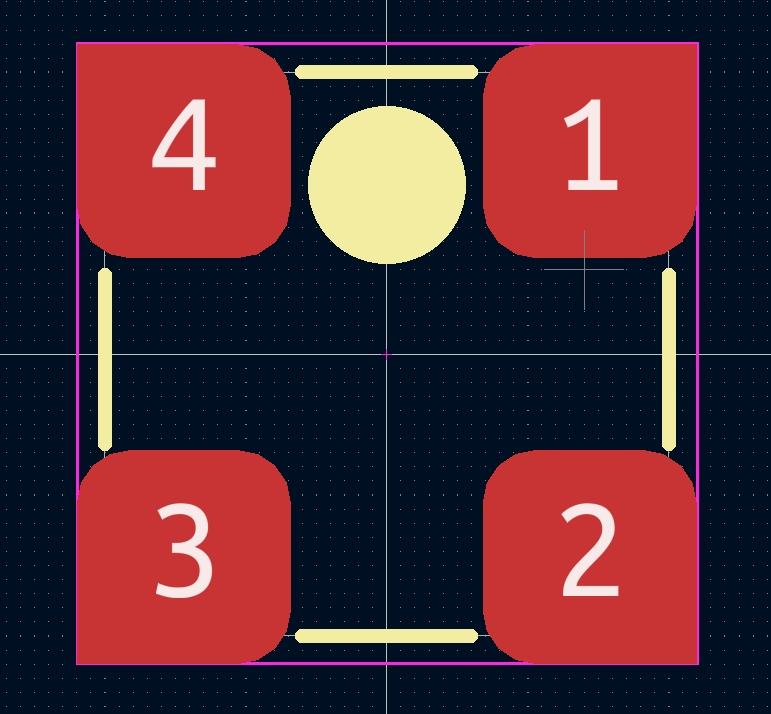
Well I'll give you a hint. The datasheet provides a BOTTOM view and you typically design a footprint from a TOP view. In other words, I'm always used to looking down onto a footprint when I am making on in KiCAD. The footprint SHOULD have looked like the one below. Notice how the pin numbering is mirrored.
(just imagine that the pads are red, okay?)
Solution: Just rotate the LED 90 degrees (and double check foot prints)
This was one of those sneaky little problems and I am pretty proud of myself for staying focused and working out the issue through process of elimination. The way things worked out, a rotation of 90 degrees is all that is needed to get the red LED doing it's thing
So pretty! Great job LED!
Problem #2 - No ground for you!
You know the LED problem wasn't that bad, I thought about things logically, tested my theories and finally converged on a solution. Things get a little fuzzy from here.
My problem was eventually this: the RP2040 would always go into boot mode regardless of the BOOT button state on powerup. The RP2040 would always present itself as a storage device to the computer.
I thought I had seen this problem before, it was like the RP2040 didn't have any flash attached to it. I had the same symptoms on Rev 1, so I thought this would be an easy fix! The strange thing is that I had fixed that problem with Rev 2. Darn! That meant I would have to think and stuff...
I was still suspicious of the flash from my Rev 1. so I focused a lot of my inital efforts there. On the Rapsberry Pi Pico schematic there is a DNP pull-up on the CS pin of the flash. I am not using the same exact flash chip so adding a pull-up on the CS line might be a good move.
The good news is that I got to use my ProtoGrid (needs more tweaking I think). The bad news is that this didn't do anything... The chip would still present itself as if there was no flash. This would happen even after trying to upload something to it. It would just eat the file, disappear and then reappear in my list of drives.
Solution: Check your footprints, make sure everything is grounded, try it anyway.
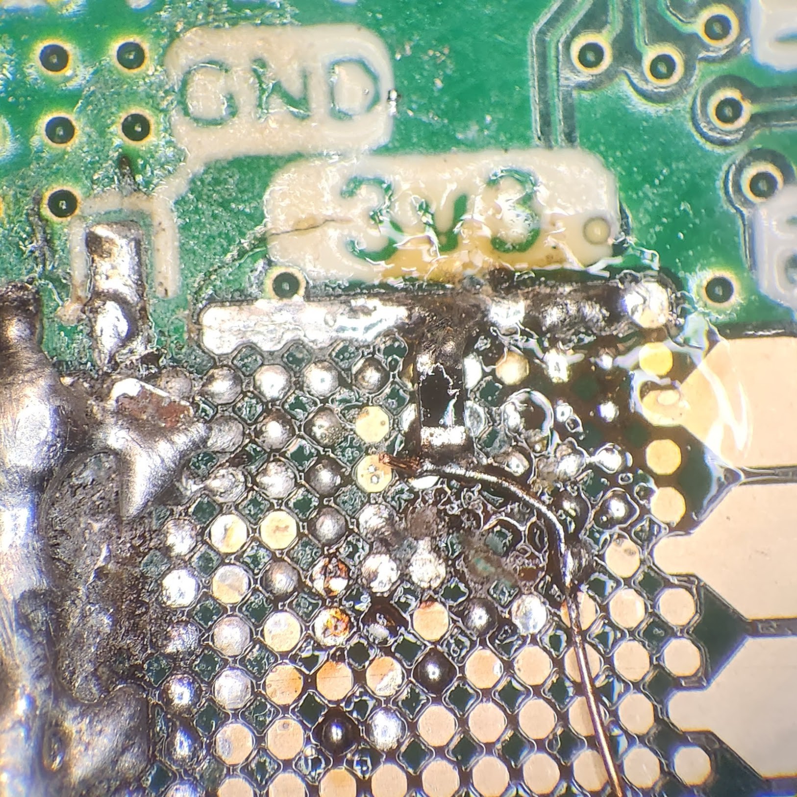
So a few different issues. The first thing I noticed that part of my ground plane wasn't connected. I had been poking around in continty mode and noticed that my buttons and my clock were on their own little island.
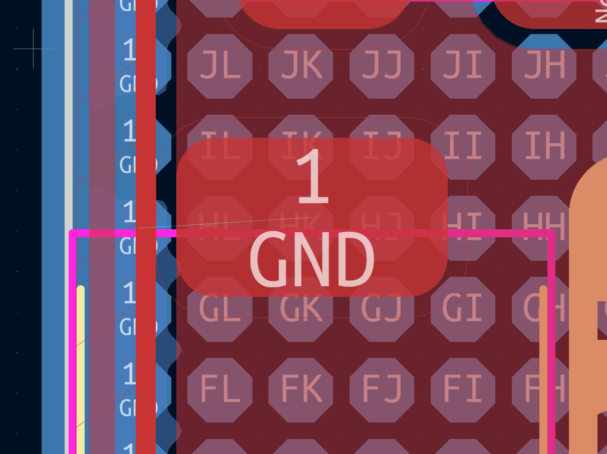
Ugh. Yup, there's a ratsnest. I do most of this work late at night so I must have missed it in the DRC.
After finding this problem my therory was that the clock wasn't actaully working but the RP2040 uses the interal ring osccilator for USB functionality so it was still showing up as a mass storage device. I dunno. Either way that was an issue, and I bodged both the buttons and the crystal to ground.
That lead to the same behavior of just perpetually remounting after being given a perfectly good firmware file. which led me investigate the buttons directly.
In the few months it took me to order them, the right angle tact buttons I had picked out went out of stock. I didn't feel like making a new footprint so I found other buttons that would fit on the old landing pattern. This was a dumb idea beacause while the original buttons I picked out only had two contact pads, the new buttons had four small leads. They were configured in the traitional tact-switch layout with the two top leads being connected and the two bottom leads being connected.
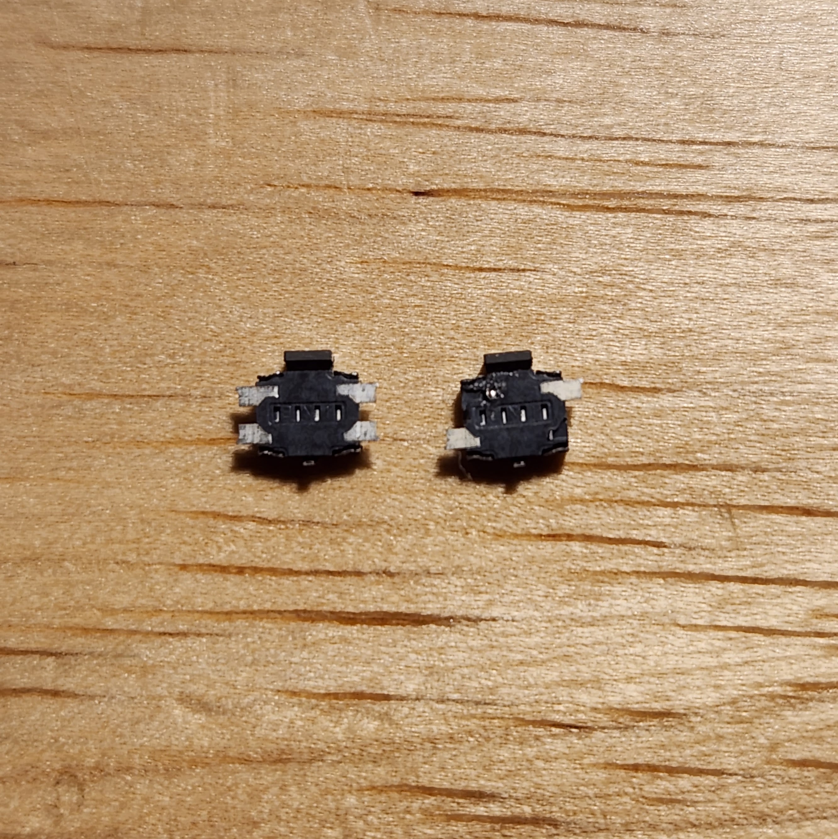
Once the ground connection issue had been resolved, the button was basically always pulled low, which would mean it would always enter into boot mode on RESET. A quick clip with some diagonal cutters and I had a button that would work! For now....
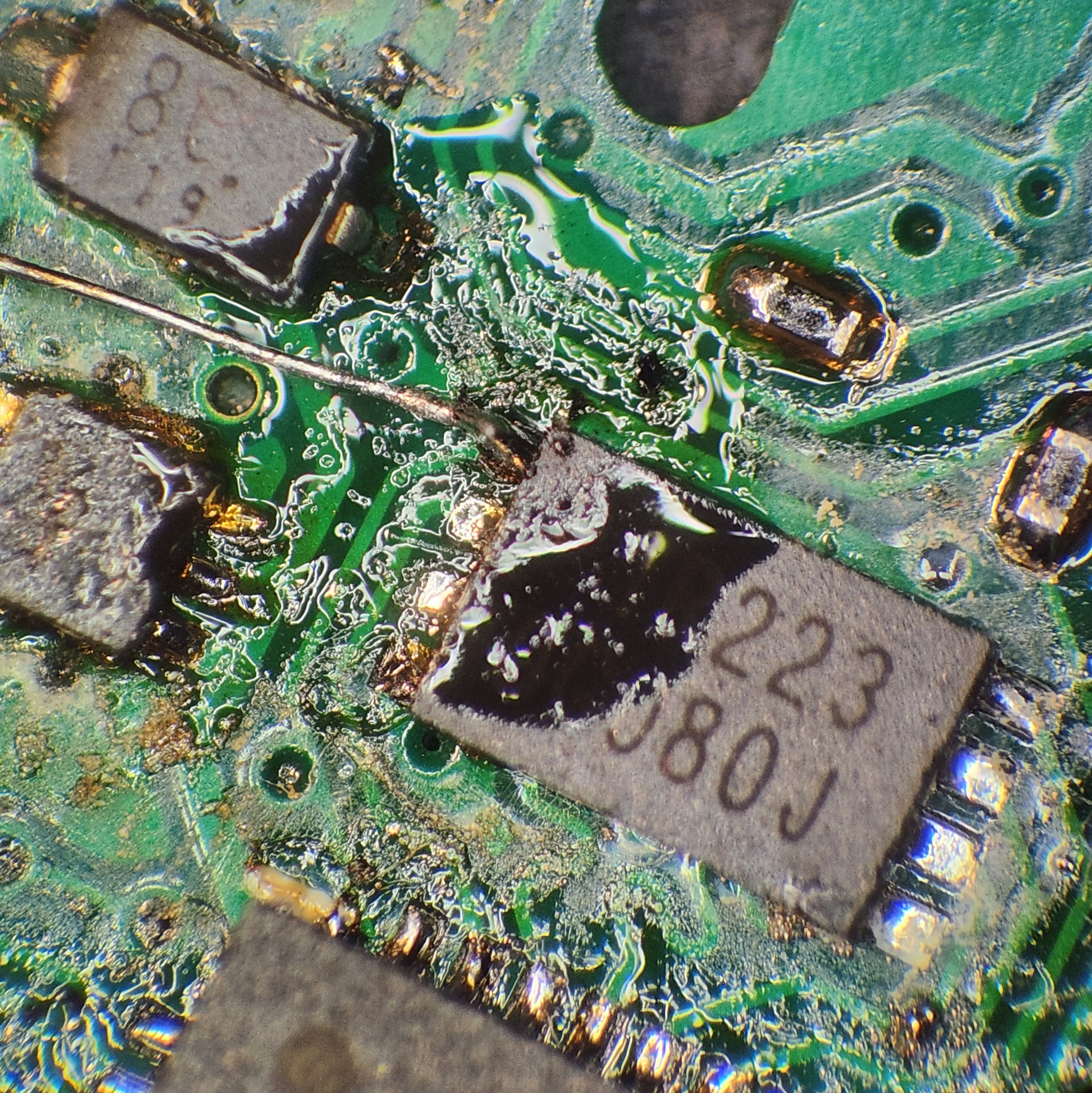
Problem #3 - Missing capacitance on the linear regulator!
This is another silly one but maybe it will be useful for someone to read. It's also getting late so I want to wrap this up quickly. For some reason, my linear regulator was putting nearly 5V onto the 3.3V line.
When I was doing all this trouble shooting, I had decided to build up a new, clean board. To save time I didn't put any decoupling capacitors on. Well that was a mistake. The linear regulator I am using is only 1.6mm x 1.6mm. WIth this size, you are paying the price of REQUIRING external capcitors. Say's so right in the data sheet.
On a fully built board with no capacitors, the regulator just refused to output anything. With the correct value of input capacitance it spit out the 5V onto the 3.3V line (most likely cooking my flash, so had to change that out). Finally, it seemed like I had too much capacitance on the output line? The regulator never raised to above 0.5V! Once I installed the recommened values things started working as intended.
Soultion: Read the datasheet and don't cut corners.
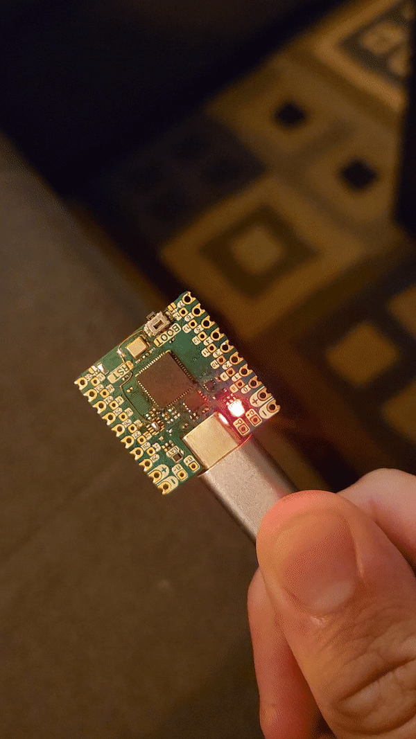
The real reason the CRAPi board started working is because I said screw it and tried programming it after fixing all these issues. Sure enough, it worked this time. Turns out it just needed the flash to not be entirely blank. The mass storage unmounted and stayed unmounted. More importantly, we got a BLINK!!!!
What's next??
A whole bunch of stuff. You'll notice that I didn't even test the LiPo charger yet (because I think there is something wrong with that circuit too!). But from there, it's just a matter of making some minor tweaks and then sending it off to PCBWay to test their services!
Discussions
Become a Hackaday.io Member
Create an account to leave a comment. Already have an account? Log In.