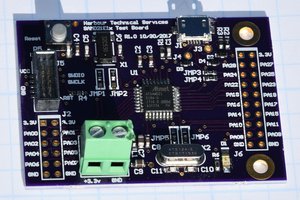
When designing this board, I knew it would have to be at least 4 layers (2 for GND and power (split voltage plane) and 2 for signals), in hindsight it would have been much better as a 6 layer board, but the price was too hard for a test run, so 4 layers it was. At first, I was designing this board for JLCPCB, so I pushed their capabilities to the maximum, pushing all their tolerances to the max (.2mm vias, .09mm traces). I knew designing this board was going to be hard, and with balancing college and work it took me about a month to design this board. Making it 4 layers was extremely hard; making me break rules that I never want to break (adding traces into the GND plane). However, the show must go on, and I wanted to get something done. Choosing what pins I wanted to go on the castillated edges took me a long time, too; I did SWD, all power lines, USB, and all ADC pins, and the rest are digital pins closest to the edge. I didn't have anyone to ask if this was smart, so I sure hope it was! Choosing what footprints to use was awkward too. I've never designed boards smaller than 0402 parts, but I felt I could be steady enough for 0201 and the added benefit of having more room for traces was a massive plus.
For part selection, I used almost all 0201 passive parts, excluding the two 0603 decoupling caps for the 3v3 LDO. Speaking of the 3v3 LDO, it is the smallest one I have ever seen (1x1mm) (https://www.lcsc.com/product-detail/_Richtek-Tech-_C147954.html), giving 300mA, which is plenty for this board plus anything extra that needs a 3v3 supply. Finding the crystal and QSPI flash was easy enough, find the smallest part, ensure it fits the specification in the RP2040 datasheet and application notes, and press buy.
For assembly, I had the stencil from JLC, which I used for assembly with the OshPark boards. I used my lead-free solder paste from Aim, which is very, very expired; having new stuff would have made the assembly process a lot easier, but I digress. Using the finest tweezers I have I assembled the top side of the board, including all 0201 parts and the 1x1mm LDO. For soldering, I had the option of using my reflow oven or a hot plate, I opted for the hot plate because the board is so small for a whole reflow warmup. For soldering the RP2040, I made a 3D-printed jig for holding the soldered board off the bench and used the stencil to lay a layer of solder paste on the back. After placing the RP2040, I soldered it using hot air at the lowest wind setting possible to prevent reflow on the other side of the board.
After all of this, the assembly was complete. I showed off this board to the other engineers at my job, and they were all equally astonished at the size of the board with the capabilities that it offered. I made a breakout board that powers the board and breaks out all data lines, and this will be here in the next few days to demonstrate the board working.
 Bharbour
 anfroholic
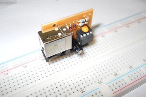
 danjovic