 jimshortz
While it's fun to play with a keypad, GPIOs, and 7 segment displays, you really can't do much without some more RAM. In particular, I wanted to be able to run some vintage Altair software and do the normal "computery" things. So, after handling the basics I set about adding significantly more RAM and a real serial port.
As described in Table 3-4, Intel provided two options for the bus expansion - all addresses or upper 32K. While having the full 64K to work with sounds appealing, there is a big caveat - you have to remove all of the existing RAM, ROM, and keypad chips. If you are going to lose all of the special things that make it an SDK-85, you might as well just build your own board with an 8085 on it. It would honestly be easier.
First, a word about project goals. I strive to keep this system as close to "period correct" as possible. You won't see ethernet controllers, Raspberry Pis, or other modern wonders tacked onto it. However, 1970s RAMs were very small and narrow. 32K in those days likely meant adding sixteen 4116 DRAMs along with refresh circuitry. This SDK-85 appears to have exactly that. This is just not something I want to undertake, so I have made a concession and am using a more modern single-chip 32K static RAM (the 62256 type). The system will behave exactly the same (except for being slightly faster) and this is a reasonable compromise for convenience. Also, I don't want to consume the entire prototype area with RAM.
Given my difficulties with the "bit bang" serial port built into the 8085, I also wanted to add a real UART. I chose the 8251 because it was an Intel part from the same time period that would have been used on other 8085 systems. Also, I had one :-)
Intel made it very easy to add things into the upper 32K. My glue logic is implemented in a single 74LS00, with one gate to spare The RAM is enabled if A15 is high and IO/M is low. The UART is enabled if A15 is high and IO/M is high. The 62256 and 8251 use Intel-style /RD and /WR lines, so no additional glue was needed.
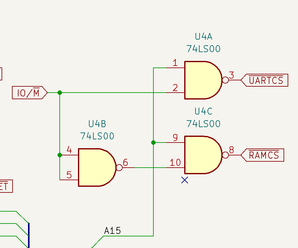
Fig 1 - Super Simple Glue Logic
I also chose to do this part using wire wrapping. This is to recreate more of the vintage experience, but also allowed me to incrementally add upgrades and easily change things around in the future. I did not solder the chips down, so that all of this could be removed in the future to return the board to museum quality.
I started by wiring in the RAM. This was very straightforward and worked correctly the first time. To test it, I simply used the keypad to punch data into 8000,8001, and FFFF and read it back. I eventually wrote something to write the old 55 AA pattern and test every bit. No problems encountered.
The UART, however was a different story. I used this vintage INS8251 from Radio Shack that I had in my junk box:
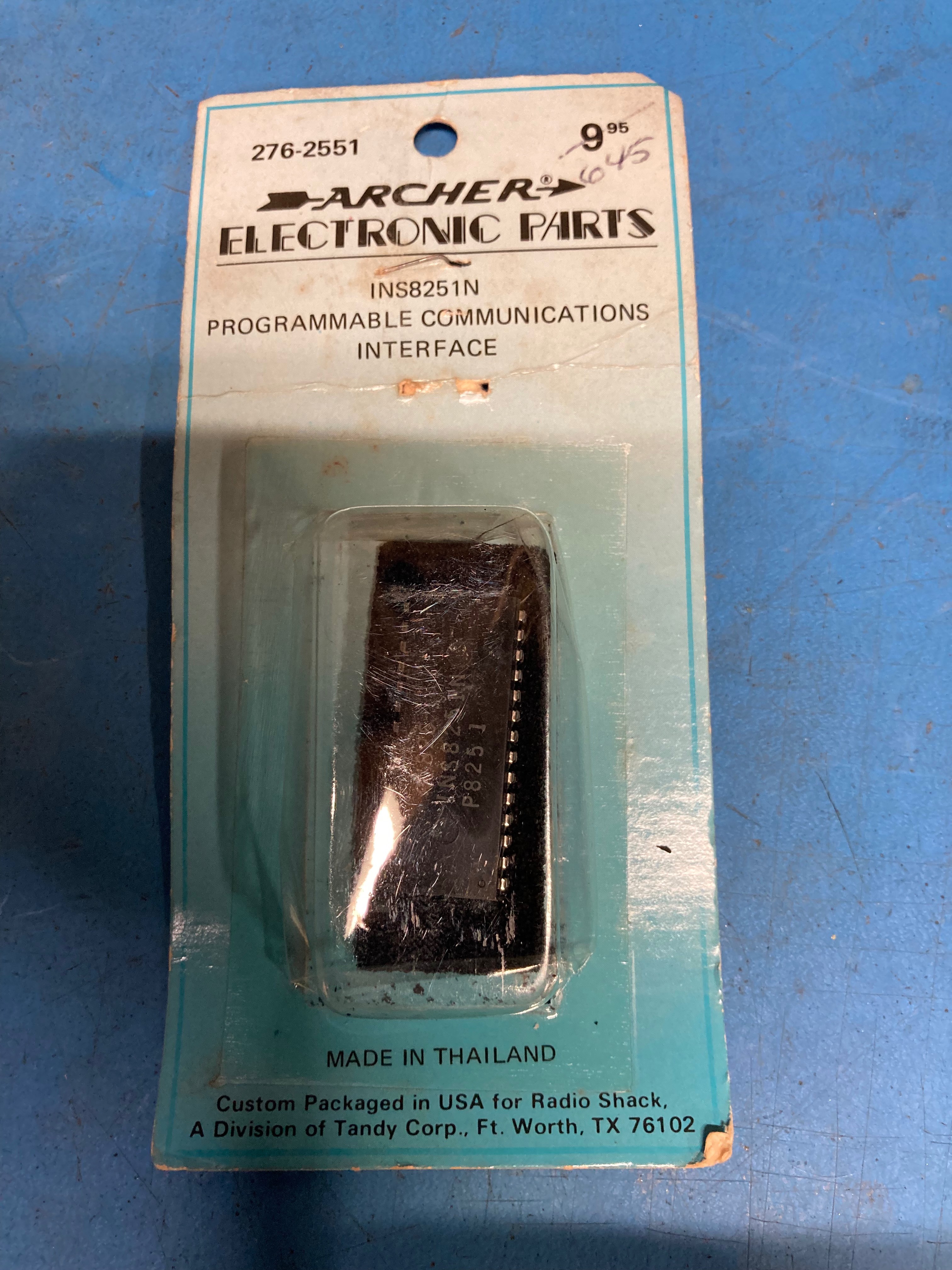
Fig 2 - Vintage UART
When I attempted to read and write the ports, nothing worked. I tried numerous troubleshooting steps for days. Eventually I intentionally swapped its CS line with the RAMs so that I could access the UART as a memory location and the RAM as an IO port. RAM as I/O worked fine, so I didn't have any fundamental misunderstanding of how the IO ports worked. But when I would read from the UART I would get back the port address (80 or 81) as data. What the heck?
Eventually I started looking at the /RD and /WR pulses on the scope and that got me thinking. I re-read the datasheet for the INS8251 and discovered it expected a 430ns read pulse width. Since the SDK-85 uses a 3.05Mhz clock, I was only getting a 327ns pulse. Believe it or not, this part was too slow for the SDK-85. So, I ordered a genuine Intel 8251A (320ns clock pulse width), installed it, and everything worked!
One difference between older UARTs (8251, 6850, etc) and modern ones (16550, FT232RL) is that modern UARTs include programmable baud rate generators. It seems unthinkable to have your baud rate set by DIP switches or jumpers, but many 1970s computers worked that way. Realistically, you are going to choose the fastest baud rate your terminal/computer can do and stick with that, so it's not a big loss.
My original plan was to use the timer output from the second 8155 as the baud rate generator, thus retaining programmability. However, during the INS8251 kerfuffle I switched to using an external signal generator. This was a good choice because it gave me an easy way to experiment with different baud rates (I wasn't sure 19200 would work). Also, it made the code shorter (which I have to type in on every boot) and freed up the timer to do other things.
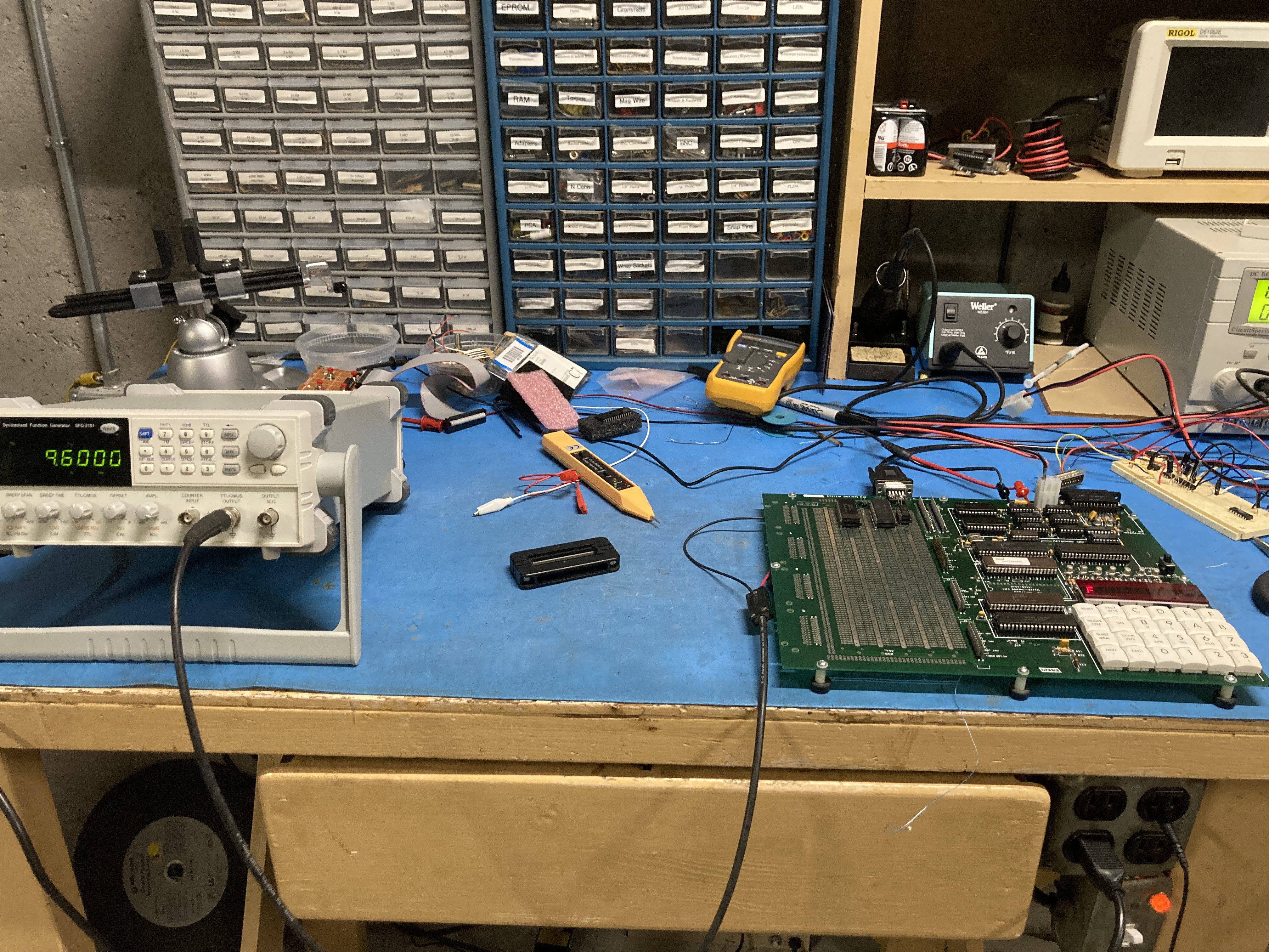
Fig 3 - Using the signal generator on a junky bench.
I wrote a very simple loader that could be keyed in. It would accept 8 bit bytes from the port, write them into a memory address, increment the pointer, and wait for the next byte. Once all bytes have been sent, you hit RESET to break out of it. You can even examine the H and L register after reboot to see how many bytes it wrote.
Unfortunately, I ran into issues downloading all but the smallest programs. I would get framing errors. I tried lowering the baud rate (very easy to do with the external generator) but still had issues. While it's easy to dismiss this as "par for the course", I have numerous vintage computers that can receive back-to-back bytes at high baud rates without incident. In particular, my Apple II can receive at 115200. A byte at 9600bps is roughly 1ms, during which time the 8085 can execute hundreds of instructions. A MOV, INR, and compare are just a few dozen T-states.
The 8251 gets its baud rate from external signals fed to the TxC and RxC input. It does include internal dividers that allow TxC and RxC to be either 1, 16, or 64 times the desired baud rate. To keep things simple I was using x1 mode. In a last ditch effort I decided to try x16 mode. Suddenly, my framing errors disappeared. I was able to download 8K programs flawlessly and repeatedly.
My hypothesis here is that there were slight differences in the baud rates used by the computer and my signal generator. The x1 mode must have only given the 8251 one opportunity to sample the input signal. After enough back-to-back bytes were sent, the start of frame would drift away from what the 8251A was expecting. Feeding it a 16x signal gives the 8251A sixteen chances to see the start bit transition and thus allow it to resync even during a long run. I have no idea how the 8251A works internally - I am just basing this on my experience in designing a Verilog UART.
With a working serial port, I was able to do lots of software experimentation. To be honest, the signal generator acted as my BRG for several weeks. Eventually I decided to build a BRG onto the board. For this I made a really simple design. A 2.4576Mhz TTL oscillator drives a CD4040 12 bit counter. You connect the appropriate output to TxC+RxC depending on the desired baud rate. This could also be done with a jumper block, DIP switches, or a rotary switch, but I just used a different colored wire wrap wire to keep things easy.
There was also the problem of voltage conversion. A standard RS-232 port uses +/-12V, but TTL is 0/5V. The MAX232 is the old standby for solving this problem and I used one on my current loop converter. For phase 2 I opted to buy a pre-built converter from Amazon that included connectors. It just happens to fit nicely on the top of the board and is soldered onto wire wrapping pins. I think this makes for a very neat presentation and offers acceptable mechanical strength.
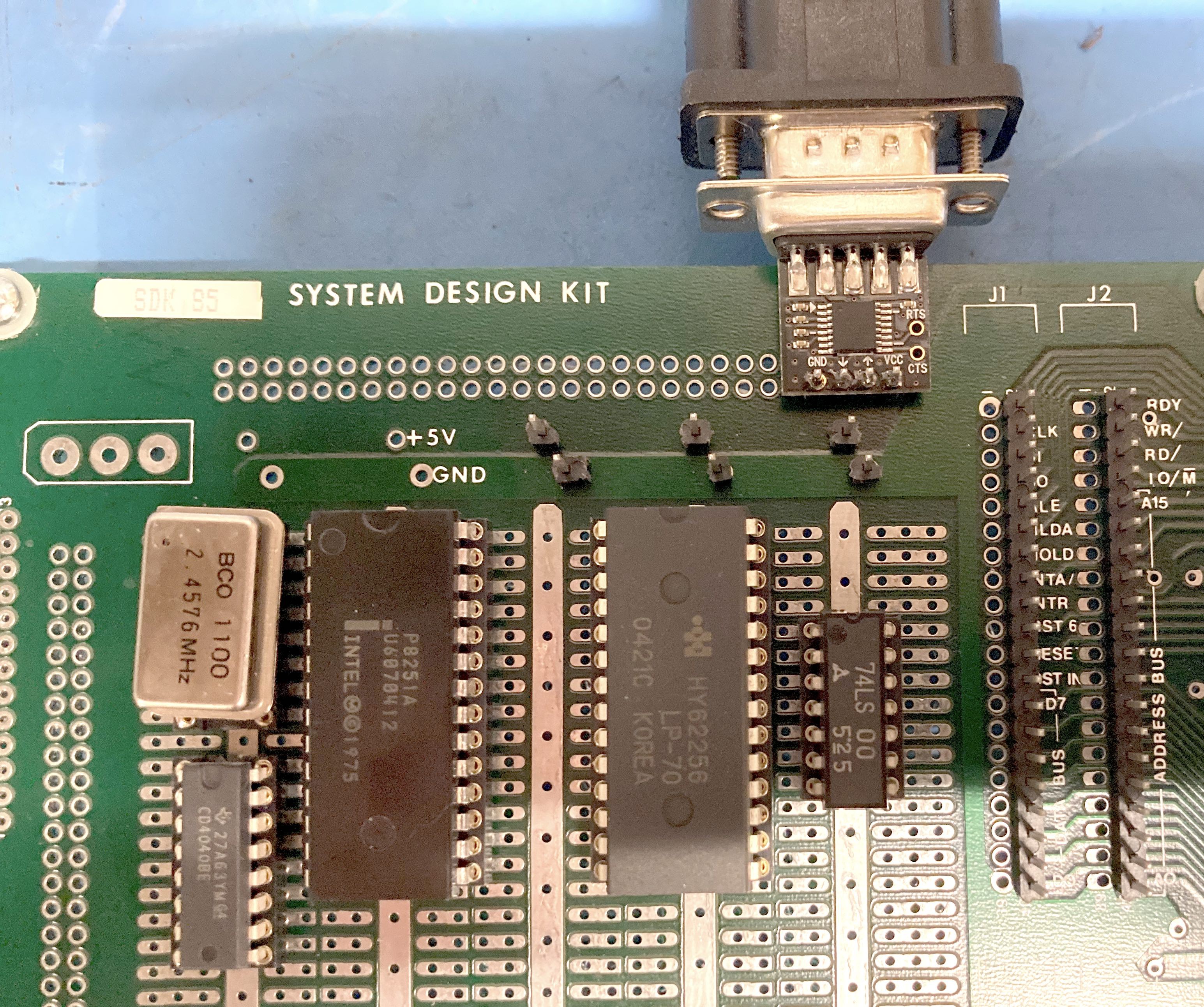
Fig 4 - Finished Product
With this design, the UART is available on I/O ports 80 and 81h. However, the entire 80-FFh range is tied up due to the very simple glue logic. To add additional I/O chips, we need to have additional glue logic. I believe a 74LS138 would nicely divide this range up among 8 devices. The memory space is also locked to a single device, but since the 62256 covers the whole address space, I don't see any reason to change. This is the primary reason I am choosing to add a second 8755A EPROM to the main part of the board rather than using a larger, more generic ROM. The on-board 8755A would sit in the lower 32K address space allowing maximum RAM in the expanded space.
The schematic is available in the files section as a PDF and in the GitHub repo as a Kicad file.
For the next installment we will switch gears and talk about the numerous software possibilities this upgrade opens up.
Discussions
Become a Hackaday.io Member
Create an account to leave a comment. Already have an account? Log In.