 nijichichi
Introduction
In general, RF circulator is well-known as a passive, non-reciprocal multi-port device that works in radio frequency (RF). When RF signal is input from a port on RF circulator, it can only propagate to the next port. Most of the passive RF circulator consist of a magnetized ferrite material. However, one can realize a non-ferrite RF circulator by using active devices such as varactors, transistor and operational amplifier (op-amp) [1,2].
The purposes of this project are to explain that how op-amp based active circulator works, and to validate that active high-frequency circulator can be realized by using current feedback op-amp (CFOA) and low-cost FR-4 substrate. CFOA is usually used for high speed or high frequency applications.
Principle and Design

Fig.1 shows 3-port basic circuit of op-amp circulator. There are three differential amplifier circuits assembled from op amps and external gain-setting resistors Z1 - Z5, and they are connected to RF port 1-3 with load Z0 respectively.
At first, to determine the resistor values, we assume that the top-left switch in Fig.1 is shorted to ground and resistors Z2 and Z4 are much higher than Z0. In this case, impedance matching condition for port 1 can be applied as below.
...(1)
The differential amplifier including OP1 is actually regarded as a inverting amplifier circuit because the inverting input terminal on OP1 is shorted to ground through Z5. Therefore, the relationship between input voltage vi at port 1 and output voltage vo on OP1 is given
Calculating voltage divider ratio, voltage vi' at port 2 is
The voltage gain between port 1 and port2 is found as
![]()
...(4).
For simplicity, one choose unilateral gain G=-1 as
![]()
...(5).
Next, output voltage vo' on OP2 can be expressed as follow.
Also, output voltage vi'' is given as
![]()
...(7).
Consider the RF circulator has the isolation response from port 1 to port 3, output voltage vo' on OP2 should be zero from (6) and (7). Therefore, you may choose the below condition so that vo' is zero.
The output voltage vo'' on the differential amplifier including OP3 becomes zero because input voltage is zero too. This means that shorting the left-top switch in Fig.1 to ground is equivalent to connecting to OP3 output.
Although port 1 is excited as shown in Fig.1, it is also same that either port 2 or port 3 is excited.
Design
To achieve high frequency performance, current feedback operational amplifier ADA4860 is used as op-amp. Note that external gain-setting resistors should not have too high resistance so as to obtain high frequency response.
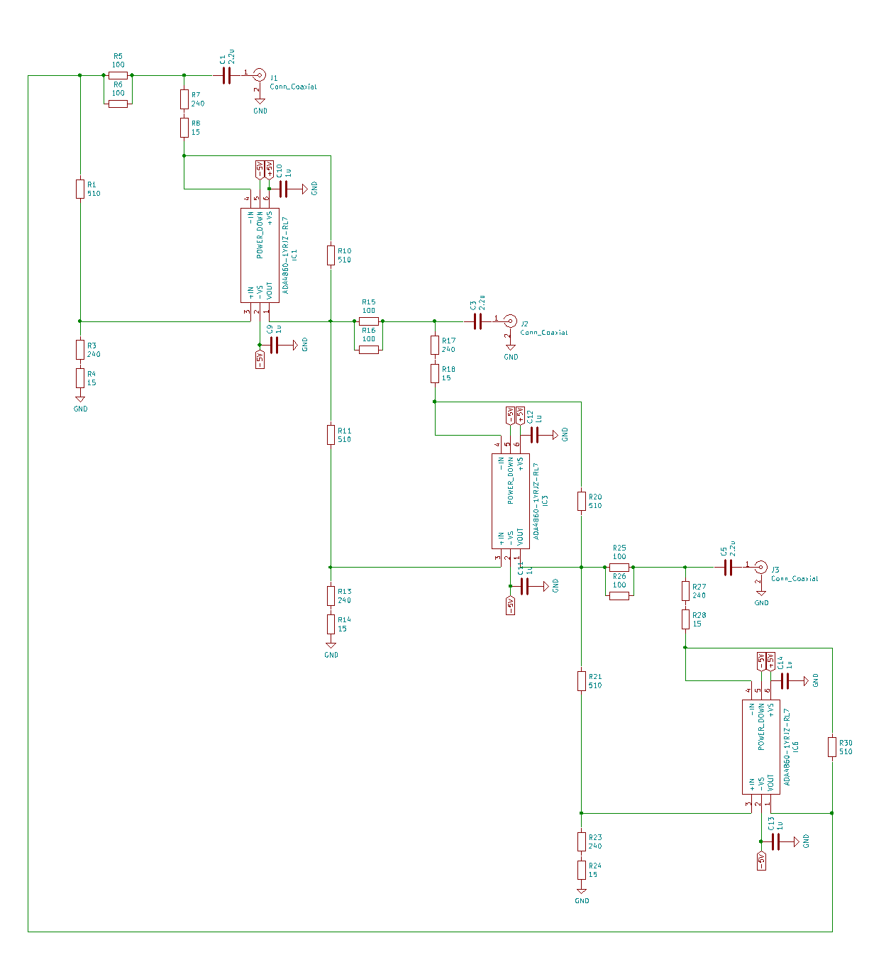
Fig.2 is circuit schematic designed in this project. These gain-setting resistor values are given in the table below.
| Z0 | 50Ω |
| Z1 | 50Ω |
| Z2 | 255Ω |
| Z3 | 510Ω |
| Z4 | 510Ω |
| Z5 | 255Ω |
Measurement

Fig. 3 is 2 layer PCB prototype which has 3 SMA ports and 3 differential amplifiers including CFOAs. these amplifiers are connected with microstrip-line each other as shown in Fig. 3. Note that two linear regulators are not used in this evaluation although it is mounted at the center of PCB. PCB material is FR-4, and the thickness of substrate is 1.0 mm. This PCB has been designed with open source EDA/CAD software KiCad and fabricated by low-cost custom PCB manufacturer PCBWay. S-parameter has been measured with LiteVNA to verify the characteristics as RF circulator. However, LiteVNA only allows measurement of S parameters s11 and s21 of DUT. Therefore, two S-parameters of 3 port RF circulator are measured in turn, while another one is terminated with load.

Fig.4 is s-parameter measurement of the circulator. Insertion response in S13, S21, S32 has been confirmed below about 200MHz....
Read more »