 Ted Yapo
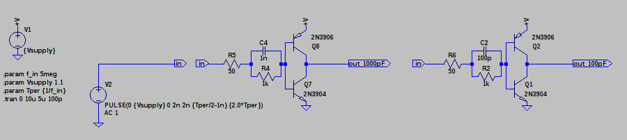
I stayed up pretty late looking at this stuff - it just didn't make sense. Finally, after playing with the simulations, I found something. The complementary NPN/PNP pair can switch very fast if it is switched continuously - like with a 50% duty cycle pulse. This somehow keeps both transistors biased, or keeps them out of saturation, or something, that allows them to switch very quickly. After a period of time this "magic quality" wears off, and they switch slowly again. I don't have a full explanation yet, but I've seen it in simulation and on the hardware now. I started with the simple inverter circuit again: here simulated with 1 nF and 100 pF caps:
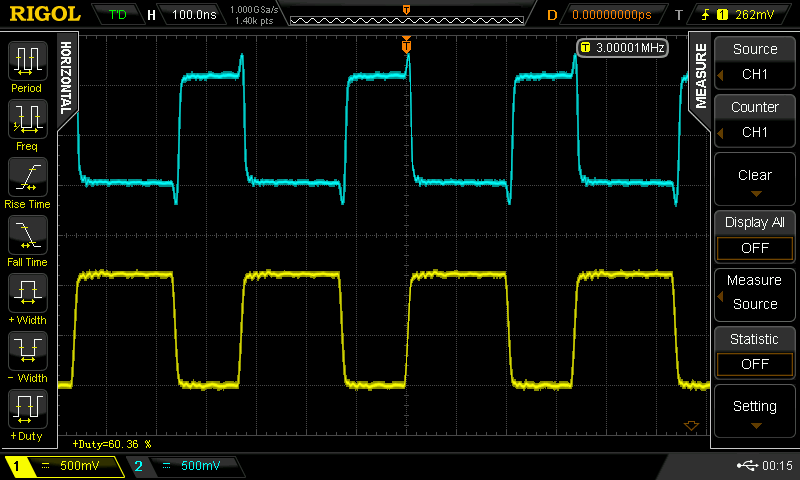
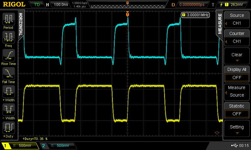
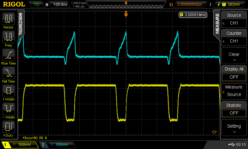
when you drive the 100 pF cap version with a 50% duty cycle square wave, you can get it to go 25 MHz (the limit of my current testing setup). With duty cycles other than 50%, the waveforms fall apart. Here are some scope shots for a 3 MHz input with various duty cycles. Yellow (lower trace) is the input to the inverter; cyan (upper trace) is the output.
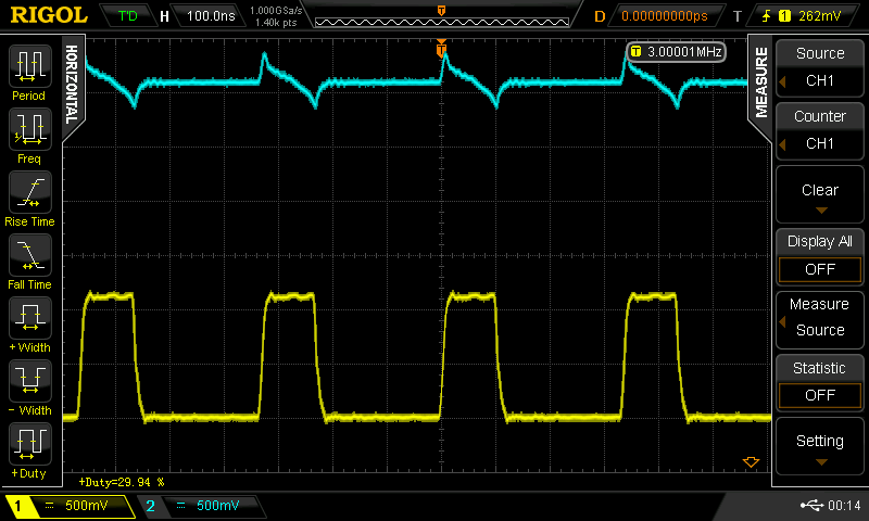 30%
30%
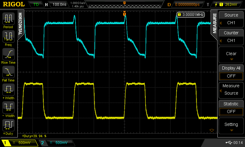 40%
40%
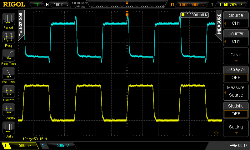 50%
50%
 60%
60%
 70%
70%
 80%
80%
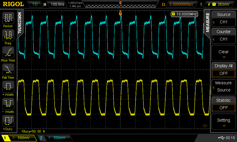
This is not just a case of minimum pulse widths - for example, here's the same circuit driven at 10 MHz with 50% duty cycle. The high time and the low time are both shorter than the 30% and 80% duty cycles above, but there's no problem at all with the output:
The same thing happens with the 1 nF capacitor, just at different frequencies. This effect is also present in the ring oscillator, which naturally assumes around a 50% duty cycle, so it is able to oscillate very quickly.
Something is happening in the transistor pair that I don't understand. I don't think the effect is really due to the duty cycle - I suspect that a recent pulse makes the pair faster for a period of time. If another transition happens within this window, the pair will remain fast. Once the effect has worn off, the pair will be slow for the next transition. I can't fully explain what is happening inside the transistors yet, but I see the same effect in LTspice, where it's much easier to make measurements, so I have a shot at figuring it out.
The real bummer is that this invalidates all the previous speed testing. I haven't fully re-run the tests yet with isolated pulses instead of square waves, but a quick look at the scope puts the propagation delays in the 25-35ns range. It's not quite as bad as a CD4001, but it's no match for even the 7404.
Discussions
Become a Hackaday.io Member
Create an account to leave a comment. Already have an account? Log In.
Is this the same effect that Tim writes about at https://hackaday.io/project/170697-evaluating-transistors-for-bipolar-logic-rtl/log/179154-using-a-led-as-base-resistor-chaotic-ring-oscillator ?
Are you sure? yes | no
I notice the 50 ohms in series, probably for the signal generator impedance.
if you can "step over", you could find/plot the ideal input and output impedances of the inverter gate...
Are you sure? yes | no
Yes, 50 is the generator impedance to keep the simulation close to the bench work - a gate that needs to be driven from an ideal voltage source is of little use :-)
Sure, I can measure input and output V/I curves - they aren't likely to be well-modeled by a single impedance value, with the gate being so non-linear. And they'll change at high frequencies, but this can be measured, too.
Are you sure? yes | no
I can't wait to read your next log !
Are you sure? yes | no
Could Germanium diodes (0.3V Vf) help reduce the strength of the saturations ?
Are you sure? yes | no
Maybe. Germanium diodes might have a low enough Vf to be used in a DTL gate with complementary output transistors. Si diodes have too much Vf for this - I tried many times :-(
Are you sure? yes | no
Oh.... I start to understand... The issue is balanced saturation !
capacitance and other effects cancel each other at sufficiently high frequency. When duty cycle is not 50%, there is more charge on one transistor than another.
The challenge now is to prevent saturation, probably with a half-way power rail to "pull-middle" ? Could Baker's clamp also work ?
I want to believe !!!
(or else, there is still ECL, damnit)
Are you sure? yes | no
Yeah, this is what I've been thinking. A feedback resistor from the output to the input seems to work OK so far - but I haven't tested it fully. This negative feedback does reduce the gain, but also sets the bias point at exactly 1/2 the supply voltage, and prevents saturation by pulling the inputs toward V/2. Interestingly, it doesn't seem to reduce the speed. I've tried it on the ring oscillator hardware (now 30 MHz), and on the NAND gate in simulation, but not extensively yet. It seems to eliminate the problem with duty cycle.
Are you sure? yes | no
3
0
M
H
Z
!
!
!
Are you sure? yes | no
so, once again, a humble resistor saves the day...
Looking forward to reading the next log !
Are you sure? yes | no
@Yann Guidon / YGDES What would you consider a minimum fan-out? There seems to be a trade-off in choosing the resistor values - I still have a lot of testing to do, but keeping a smaller fan-out will help optimize other parameters. Things get slower with a large fan-out. I've been here before with other logic: fan-out of 2 is an absolute minimum, while maybe 5 is a minimum to stay sane during design of a large system. Of course, you can also use different R's and C's in "driver" gates when necessary.
Are you sure? yes | no
Why choose ?
If you could make a plot or a formula of "feedback vs fanout", that would be awesome :-)
Are you sure? yes | no
Isnt that the principle behind ECL? (and PECL for positive voltages)
Are you sure? yes | no
no.
The idea behind ECL is a bit complex but doesn't use feedback.
Great analysis, long but insightful :
https://en.wikibooks.org/wiki/Circuit_Idea/Revealing_the_Truth_about_ECL_Circuits
enjoy ! :-)
For my Silicon computer, i'm still torn between ECL and CBJT...
Are you sure? yes | no
Oh, I got it. All signals in the system have to be Manchester-encoded to ensure a balanced number of frequent transitions. I wonder if you can operate logic gates on Manchester-encoded signals directly??
https://en.wikipedia.org/wiki/Manchester_code
Are you sure? yes | no
yer on it!
Are you sure? yes | no
Interesting dreams you must have. You've still got the option to build a machine for processing bandwidth limited data ;-)
Are you sure? yes | no
Yes, you have your choice - you can process data slowly at low frequencies, or modulate it up to high frequencies, and process it slowly there. It's like saying the diode logic in my other project has a clock speed of 6 MHz - technically true, but that's the power supply frequency; the logic runs at 3 kHz max :-)
Are you sure? yes | no
Ah that's the trick behind your DDL logic! I spent some time browsing your docs but I didn't find a document on its workings.
Are you sure? yes | no
The workings behind the clock are in the DDL01 datasheet (page 5):
https://cdn.hackaday.io/files/11677499588768/DDL01_datasheet.pdf
The rest of it is simple - just a clock made with NOR gates.
Are you sure? yes | no
This was fun reading, and the idea is intreguing! I also liked the "datasheet style". A really nice project!
Are you sure? yes | no
Interesting effects.... Now that you mention it, I vaguely recall seeing some oddities like these when using BJT-based motor-drivers at various switching-frequencies way above their specs. (As in, they weren't spec'd for PWM, at all, but for full-on-full-off end-to-end movement of the motors).
Are you sure? yes | no
Yeah, switching and amplifying are two different things, really. These transistors have a transition frequency of 300 MHz (min), so even at 30 MHz they'd have a (linear) gain of 10. Plenty to amplify a 25 MHz signal if biased correctly, even if they can't switch fully on and off that quickly.
So, maybe at low speeds, they are doing saturated switching, but high-speed 50% duty cycle inputs bias them into the linear region, where they're faster. If this is the case, maybe there's a way to keep them in that region always - like by reducing the gain with a feedback resistor from the output back to the input. This kind of feedback reduces the (linear) gain, but stabilizes the operating point. Hmm...
You know, there might be something to this. If you think about the DC component of the input as a bias, a 50% duty cycle input has a bias voltage of exactly 1/2 of the supply. Duty cycles other than 50% have DC components closer to one or the other rail, maybe allowing one of the transistors to go into saturation, which prevents it from switching quickly.
Are you sure? yes | no
Sounds to me like there might be something in considering this not quite as regular ol' logic, but as something more like phase-shifted-logic... always run it at high-frequency, but ones and zeros might be represented as different phases, or something. You're the expert, here, with your diode-clock :)
Feedback sounds more logical, but for some reason speaks to me as slower...(?)
Are you sure? yes | no
If they're not saturating, though... doesn't that mean both transistors are on simultaneously?
Also, Wiki says "forward-active: E < B < C"... but say you're driving a second inverter from a first, and the first's collector is greater than VBENPN=0.6V, then your output is >=0.6V, which isn't low enough to turn on the second inverter's PNP...(?)
Are you sure? yes | no
What about... You inserted a 1 Ohm (or 10 Ohm) resistor between the transistors, to look at the simultaneous-conduction current ?
Are you sure? yes | no
Yes, getting a look at the currents is a good idea, but hasn't yielded anything definite yet. As long as I trust the LTspice simulation, I can probe the currents without disturbing the circuit at all - I can see current into any device terminal, as well as all voltages. So far, just a few clues. Since I see the same behavior in simulation as on the bench, it's much easier to poke around in the virtual world.
There are big shoot-through current spikes during the transitions, when there are transitions. I had seen these before, and they don't seem to matter very much.
Are you sure? yes | no
Please Ted. Stop crushing my dreams.
Are you sure? yes | no
I would hate to have someone solder up a few thousand transistors just to find out that it doesn't work. Especially if it were me doing the soldering :-)
Are you sure? yes | no