 Ted Yapo
I hadn't home-etched a board since I discovered OSH Park (first order 1/12/13). Actually, before that, I used another service that didn't do soldermask or silkscreen, only offered one size board, and made you use their proprietary layout software. I also walked to school - uphill both ways; kids these days have it easy. Anyway, my bottle of ferric chloride is at least five years old, but it still works:
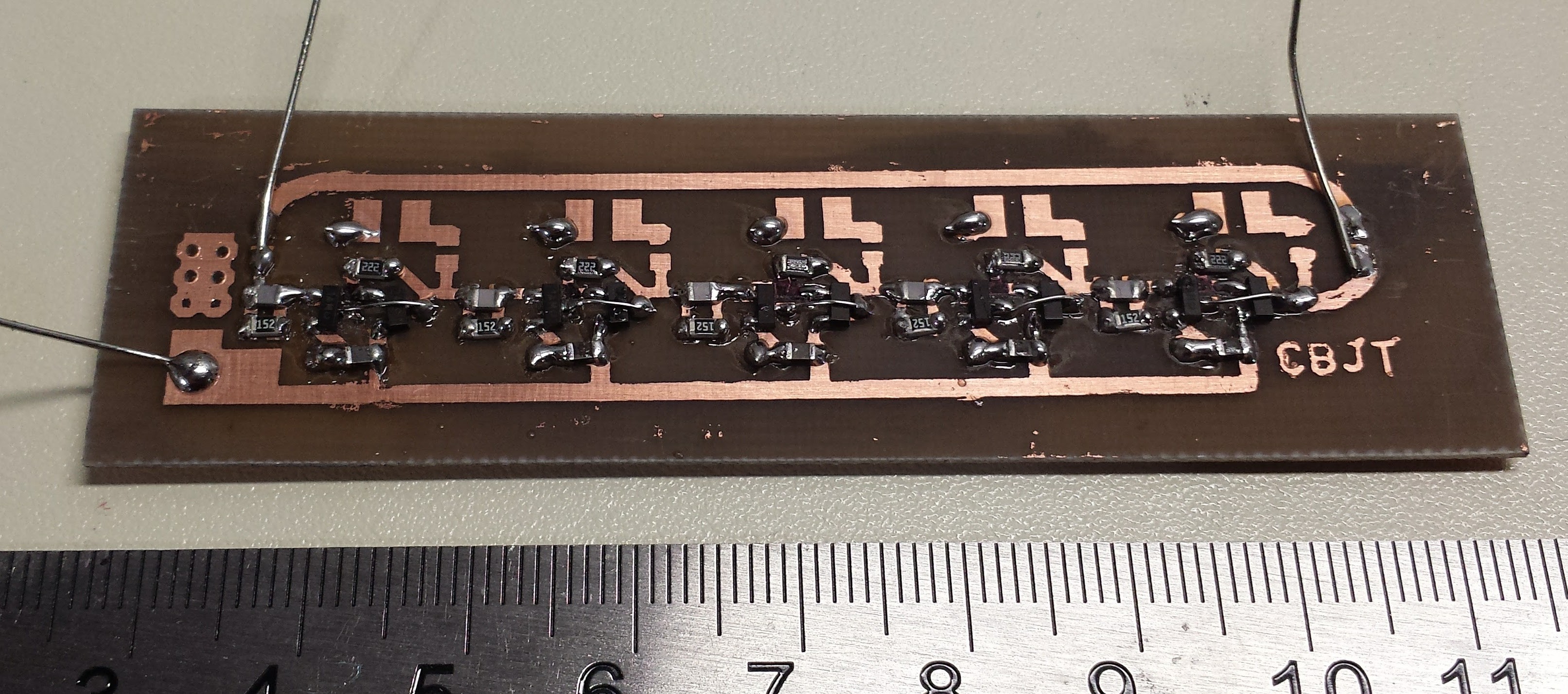
It's a 5-stage ring oscillator with MMBT3904/MMBT3906 devices and the 2R (feedback) design. I didn't have 1.6k 0805 resistors, so it uses 1.5k and 2.2k. The bottom of the board is solid copper, and ground connections are made with wire "vias" in drilled holes. At 1.2V supply, the thing runs at 30.3 MHz, indicating a propagation delay of 3.3 ns. This is significantly longer than the simulations, but not really that bad. I don't think the 1.6k -> 1.5k substitution is to blame; it didn't make much difference in the simulation - but it might be causing other issues described below.
Thinking there might be something wrong, I built a version with through-hole parts, too:
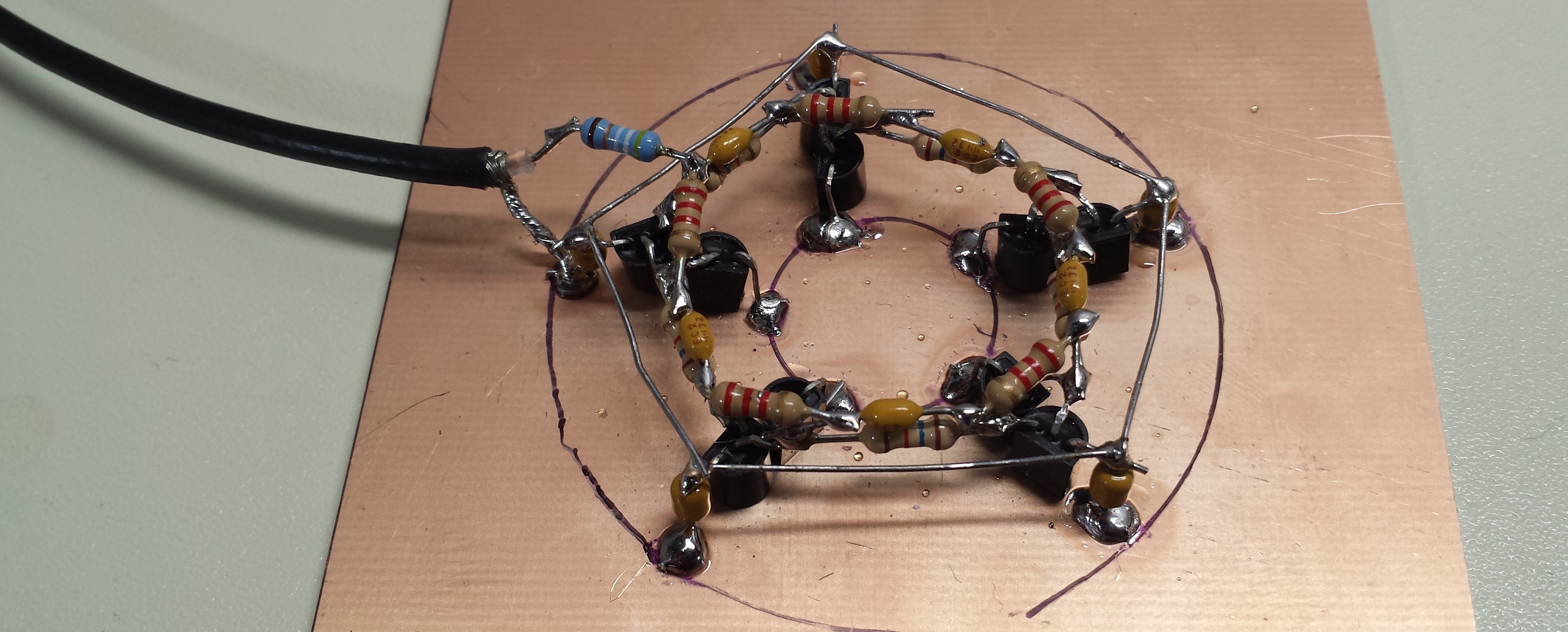
This one uses 1.6k resistors. It runs at 33.4 MHz, for a propagation delay of around 3.0 ns at 1.2V. If you turn up the voltage, you can get it to peak around 37MHz, at high current drain. At high enough voltages, the speed drops again. I can't explain the difference in speed between the two versions. The TO92's are bona fide Fairchild transistors from a reliable distributor; the MMBT's are no-names I (probably) bought on ebay. Maybe they're not the real thing? Of course, this could be layout issues, too - is that long feedback line to blame? I think it's only about 250ps long electrically. And those 1.5k R's? Hmm.
Pulse Testing
Since the output impedance of these gates is so low, and the edge rates so fast, the output of my 50-ohm signal generator isn't a good source for testing. I decided to build a buffer with a 74AC02 quad NOR (because I have a ton of them). The edge rates of the AC logic are around the same as I have seen with these CBJT gates, and I made a voltage/impedance converter network so that the output is around 1.2V peak with a 9-ohm impedance:
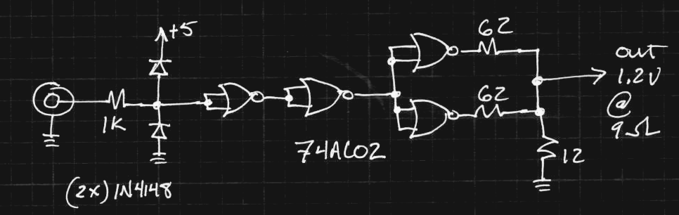
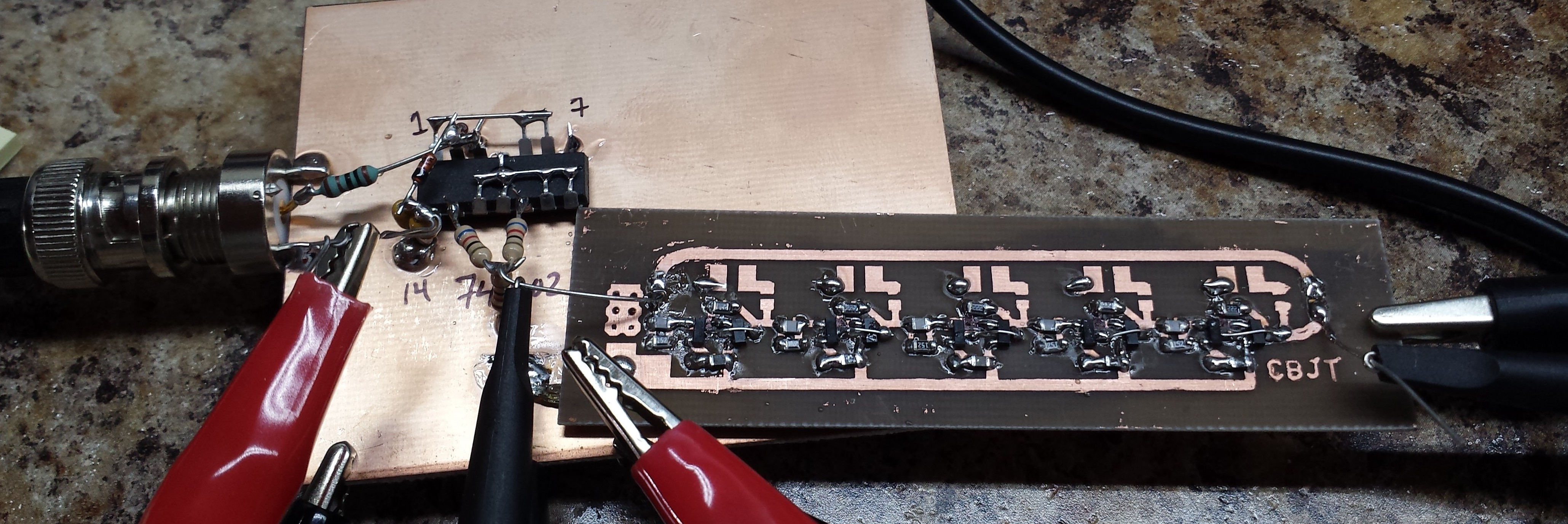
This circuit assumes a 5V supply for the 74AC02 and a 12-ohm output impedance for these NOR gates - I had previously measured around this value. Using this circuit at the output of my signal generator produces waveforms that look like the output of the CBJT inverters. Here's the adapter soldered together with the SMT test circuit:
First Impressions
So, I fired up a 10 MHz square wave input, and measured the output at the end of the chain of 5 inverters (with the ring oscillator feedback trace disconnected). Here are the waveforms (yellow = input, cyan = output):
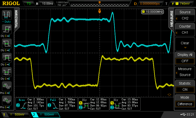
The rise time is about 2.1 ns, and the fall time 1.5 ns: fast edges. The measured propagation delay is 2.7 ns on average. This is faster than the ring oscillator measurements. You can also see that my generator at 50% duty cycle doesn't appear to be exactly 50%. Maybe the 74AC02 converter is stretching one side?
Changing Duty Cycle
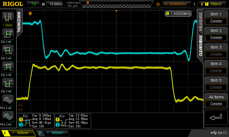
The non-feedback design had a problem with transistor saturation at high or low duty cycles. This version has its own peculiarities, namely it stretches isolated pulses. As before, a 50% duty cycle input is fine, but isolated pulses are distorted a little. In this case, the pulse (either high-going or low going) is stretched by an amount inversely proportional to the pulse width - very counter-intuitive. For example, here are input pulse widths of 18.5 and 133ns producing output pulses of 31.3 and 137 ns:
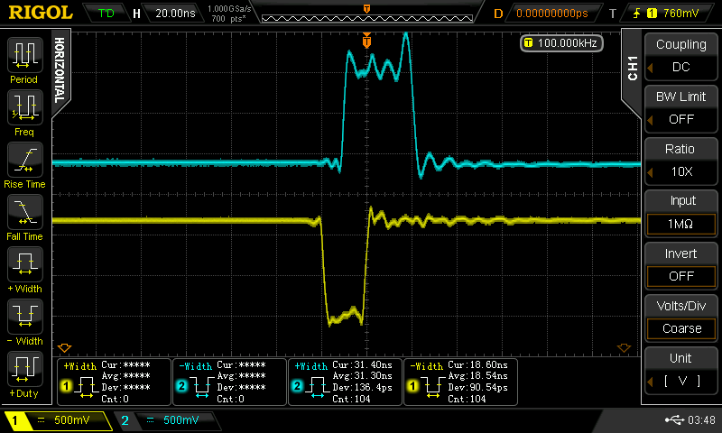
This is a stretching of 12.8 ns for the shorter pulse and 4 ns for the longer one. Bizarre. This happens for negative-going isolated pulses, too. And, it goes away with near-50% duty cycles, like before. It may be that this would be improved if I had 1.6k resistors in there instead of 1.5. I can try later with through-hole components where I have a stock of the 1.6k.
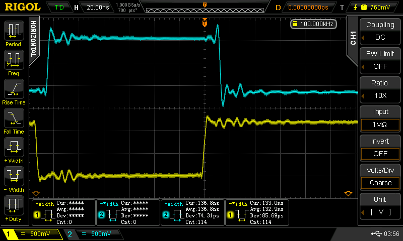
One way to look at this pulse stretching is as an additional delay. If you account for th worst-case stretch as part of the propagation delay, your design should just work. Here's that this looks like (with positive pulses this time):
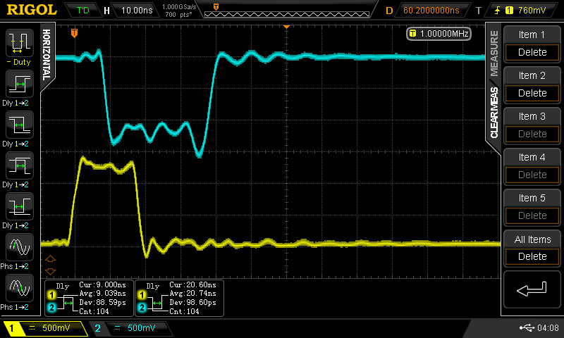
On the left, with a 20 ns input pulse, the worst case delay here is 21ns for 5 inverters, or 4.2 ns each. This pulse represents a single clock pulse in a system with period of 40 ns, or 25 MHz clock frequency. With a 100 ns input pulse (right), the delay has decreased to 2.7 ns, matching the measurement with the square wave.
It's almost like there's a minimum pulse width for the output. I collected the following data for input pulse vs output pulse width:
| Input Pulse Width (ns) | Output Pulse Width (ns) |
| 18.54 | 31.3 |
| 28.22 | 39.05 |
| 44.80 | 53.63 |
| 52.81 | 60.88 |
| 60.90 | 68.23 |
| 68.86 | 75.60 |
| 84.90 | 90.62 |
| 92.91 | 98.24 |
| 100.9 | 105.9 |
| 108.9 | 113.6 |
| 116.9 | 121.3 |
| 132.9 | 136.8 |
This data looks pretty linear when plotted. A simple regression line gives:
So, it's almost like there's a minimum output pulse width of 12.5 ns for isolated pulses. But, the stretching is reduced for longer input pulses (that 0.927 should be 1). Very strange.
I'm not sure what to make of all of it yet. Maybe moving to the 1.6k resistor will improve things? And what about 2-input gates, NAND and NOR? More things to look at.
Full Circle
So, I'm finally coming to understand why the original design we found uses a split input network and pull-up/pull-down resistors. I've been playing with some simulations, and it looks like this buys you some nice properties (less sensitivity to power supply level, higher gain, easier control of saturation) but at a price of more components and possibly another supply rail. A wiser person might have adopted that design first, but I had to bang my head against this problem until I understood how they ended up where they did. I think I'm getting close - sounds like another log is in my future.
Discussions
Become a Hackaday.io Member
Create an account to leave a comment. Already have an account? Log In.
Your pulse stretching may be due to the parallel RC network on the input of each gate. The capacitor will add a phase lag, while the resistor won't, leading to a stretched pulse when the two are superimposed.
Are you sure? yes | no
It's fun following you guys. Some hours ago I mused about how much better my PCB making autonomy was when I was a teenager than it is now. I guess I'll have to invest in some basic tools.
Are you sure? yes | no
Wow that is another awesome log :-) Thanks for all the work ! The results are very interesting...
Are you sure? yes | no