 Tamas Feher
Exploring Capacitive Touch
Introduction
In this log I'll introduce my first attempt at sensing the ball's X,Y position on a plate, using Capacitive touch sensing. The entire solution is self contained within a single custom PCB
The Appeal of Capacitive Touch
In the log BJR_LOG_03 Plate subsystem breakdown I introduced the main touch sensing technologies I considered, and landed on Capacitive touch sensing. Just to recap, it operated on the basis of detecting the change in capacitance in the panel when a finger/stylus touches the surface. This technology is used in almost all smartphones, and laptop touch pads. In our use case the sensor doesn't need to be transparent, so it can be all self contained within a single PCB.
The Design
The circuit itself if fairly simple. Here is the high level overview:
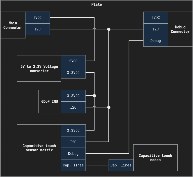
I threw in an imu into the design as well to be able to compensate for uneven floor. It might not be needed in the long run, and it doesn't hurt the prototype. The debug connector helps connecting the touch controller to a computer without having to write a driver for the device.
I used KiCad to create a prototype PCB that could be tested with the system. here is the schematics of it:
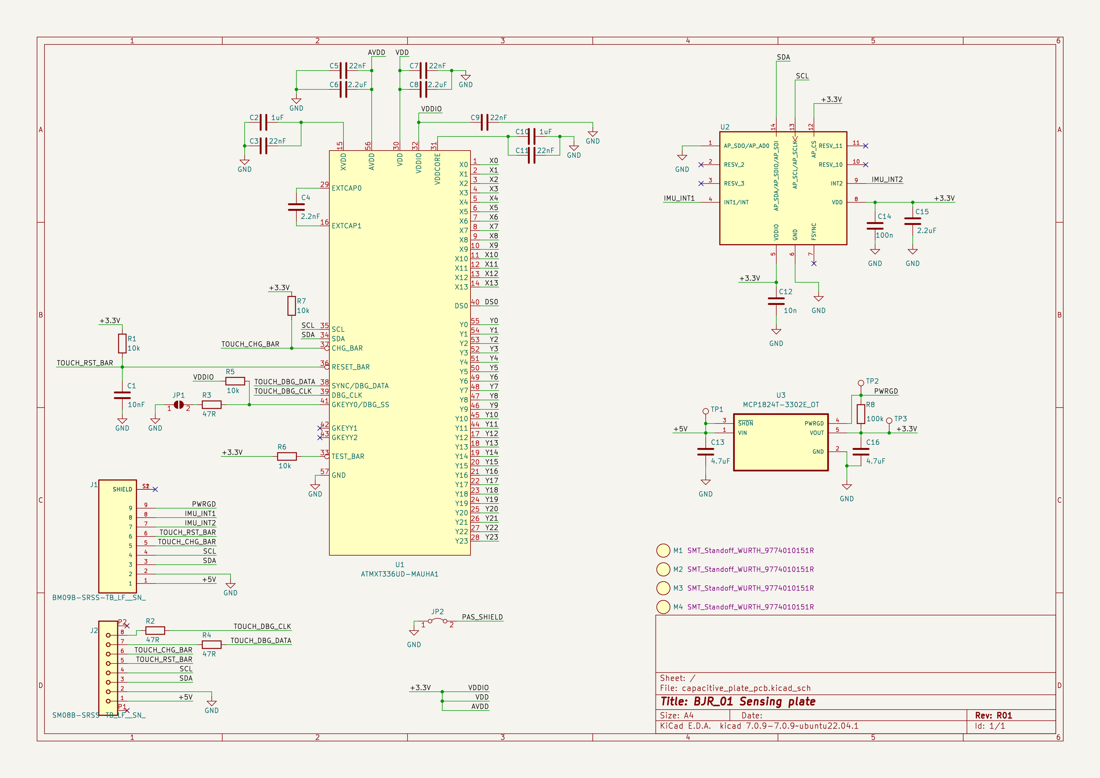
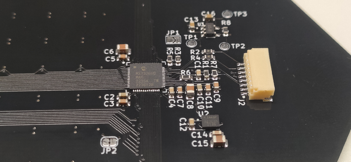
The main star of the assembly is the ATMXT336UD. It's a touch screen controller with 336 nodes from the maXTouch product family. It does all the measurement, signal processing, filtering, the whole bundle. It reports touch information on an I2C bus.
The sensing elements are arranged into rows and columns. The Columns are driven, and cycled through one by one. The rows are measured against the active column of sensing elements. This is how the 2d plane is covered with so many nodes.
A 4 layer pcb was used, where the layers look like the following:
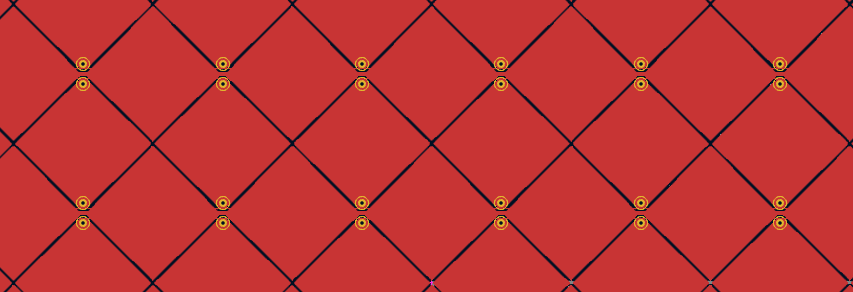
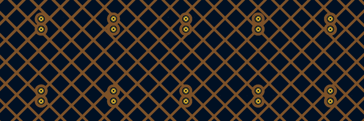
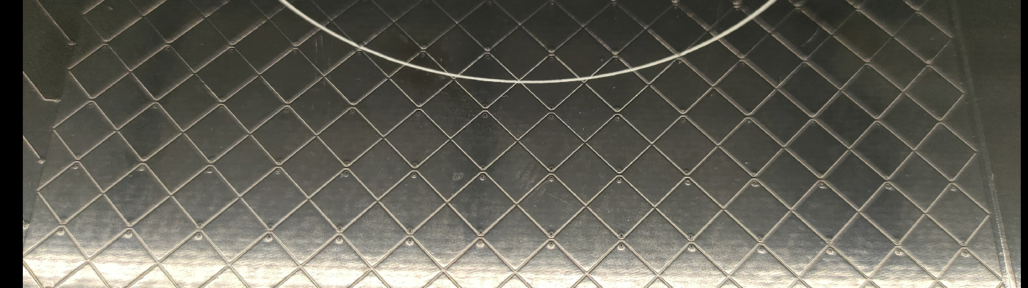
- Layer: The top most layer contains the sensor nodes. A diamond pattern was used, to maximize sensitivity of the mutual capacitance sensor.
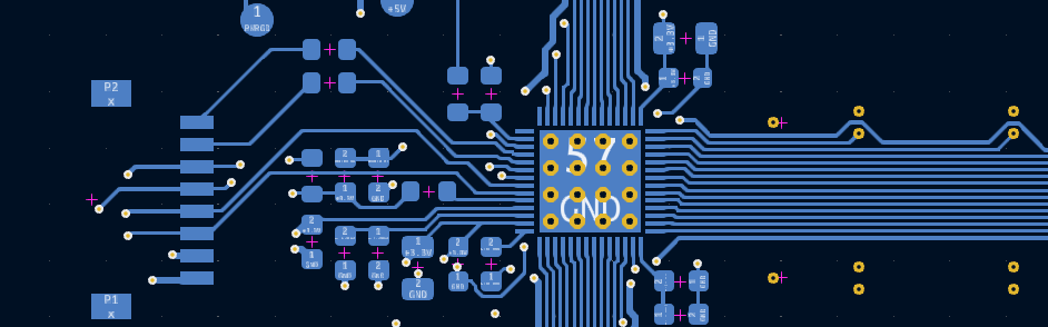
- Layer: Contains the interconnection between the column nodes:
- Layer: Creates the shielding for the sensors. A soling ground plane fill would disrupt the electrostatic field, so a hatched fill is used with 25% infill.
- Layer: Is the component and signal layer.

Some components had way too narrow pitch for me to comfortably hand solder it, so I asked the PCB manufacturer to populate the boards for me.
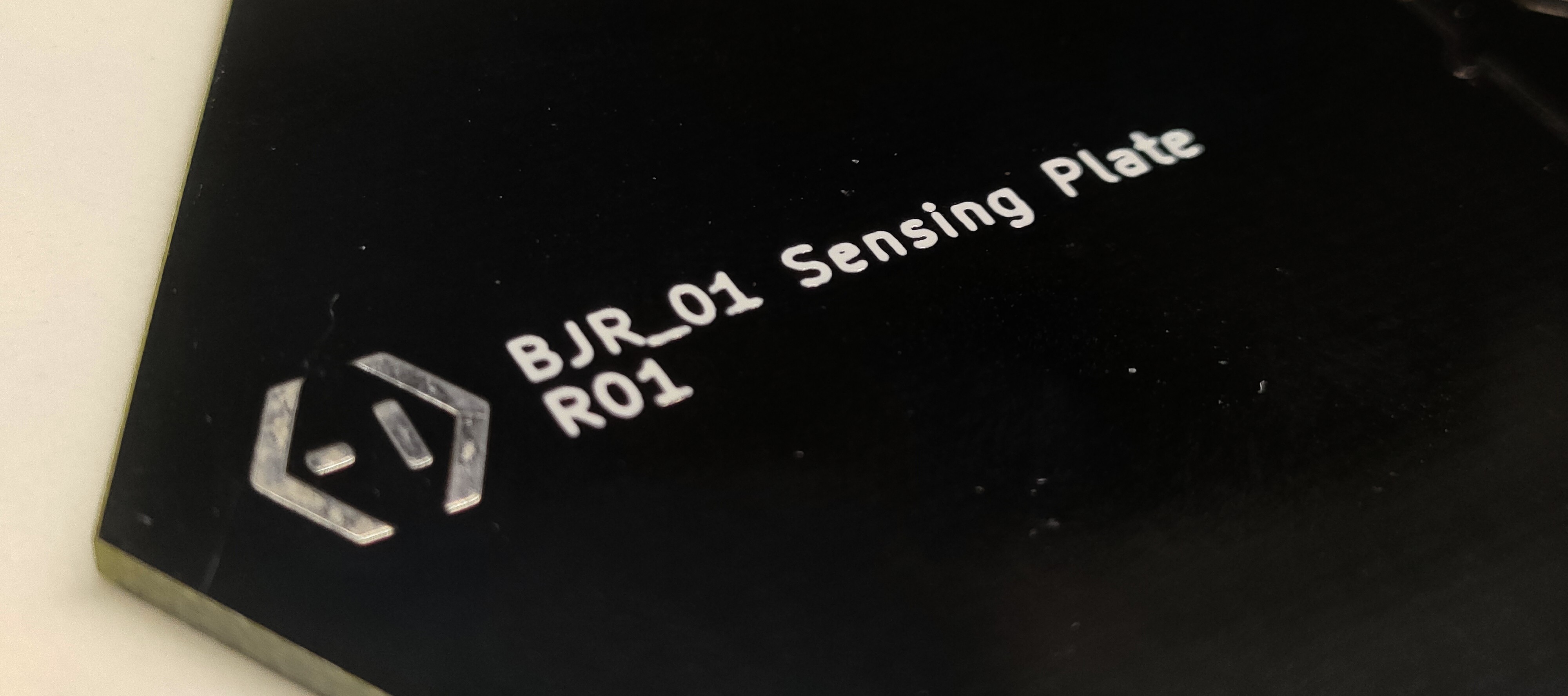
Here are some pictures of the complete board:
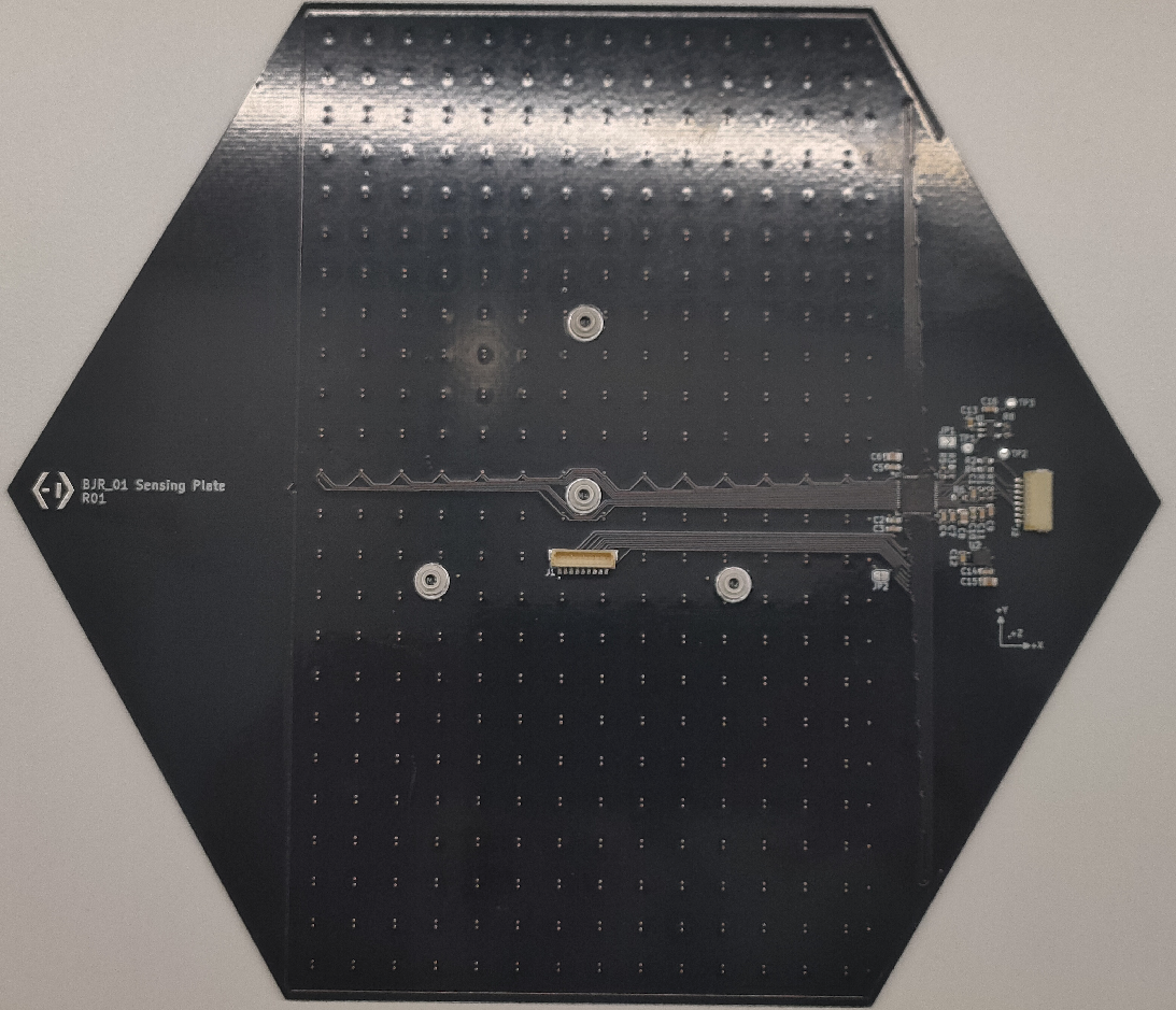
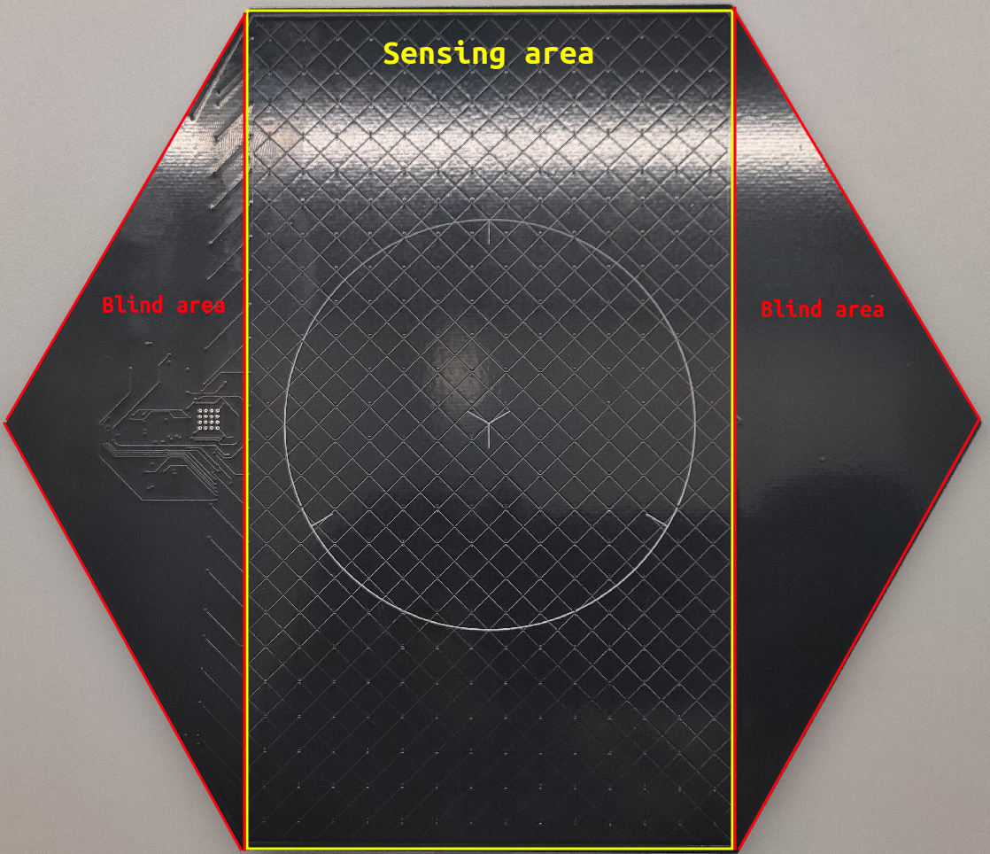
The sensing area is much smaller than the entire plate. The application note recommended to use rectangular footprint.
The next picture shows the diamonds sensing pattern.
Resources
This board was very much out of my comfort zone, as I've never used capacitive sensing before. Thankfully there are great resources available online which holds your hand through the design process with examples and application notes. The most useful resources for me were:
- CapTIvate™ Technology Guide Gives a good general overview of capacitive sensing methods and applying it to TI's capacitive inputs.
- Design Guidelines for PCB Layouts for maXTouch Controllers Helped with the layout of the components and sensing elements.
- QTAN0080: maXTouch Sensor Design Guide Gave help to tailor the design to the maXTouch product range.
Results
The next log will deep dive into the evaluation of this board. To give a bit of spoilers, the board Functionally works well, it detects human touch very well, however the touch of the ball yields very inconsistent results. We will see why in the next log.
Make sure to follow and like the project if you're interested how the plate operates in the target environment.
Takeaways
I hope this log helps show that an unfamiliar technology can be safely explored through manufacturers' application notes.
Discussions
Become a Hackaday.io Member
Create an account to leave a comment. Already have an account? Log In.