 Anders Dinsen
The IQR83 main computer communicates with the outside world through the obscure TMS9900 "CRU" interface. CRU is short for "Communications Register Unit".
The CRU interface has been described as 4096 wires but it is actually one input pin, one output pin, a clock-out signal, and a number of address bits. The pinout of the TMS9981 is shown below with the CRU and address pins that are relevant on the IQR 83.
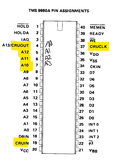
On the IQR 83 only the four least significant address pins are brought out to the outside world, but there's a thing here to note about the TMS9981: Texas Instruments numbered the most significant address and data bits number 0, and the least significant number 15. This is opposite of what most other CPU manufacturers did at the time - and obviously opposite of what everybody does today. Blaupunkt/BOSCH, however decided to number the data- and address bits in the conventional way so in the schematics of the radio, the numbering of the bits are like we're used to today.
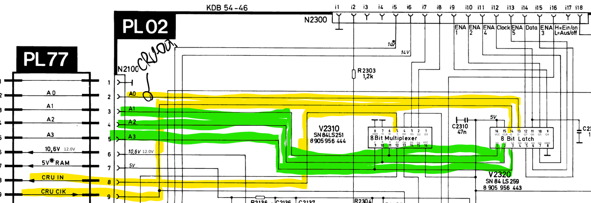
That's why I've hand written A0, A1, A2, and A3 on the pinout and for the rest of this log entry, I'm using the numbering used by Blaupunkt/BOSCH. Below is the schematics for the bus board connecting the CPU board to the outside world with the relevant I/O lines highlighted:
Another thing to note is that while A0-A3 is brought out, but A0 is used for the CRU-OUT signal, so the address pins in use for CRU I/O are A1, A2, A3.
Confused? I hope not. Also, I think it makes sense once you see the software and hardware implementations.
The idea behind the CRU interface is that the CPU addresses one I/O bit at a time: The CRUCLK latches out whatever bit is on A0 as to whatever address is selected. Decoding is simple and requires only an address decoder and a bit addressable latch. This can be implemented in standard TTL circuits. An 74LS259 8 bit latch for CRU-output is used in the IQR83.
For input, the situation is a little different: There's one common CRU-IN signal shared by all input devices. However, only the one being addressed on the address lines must output a signal to CRU-IN. The CPU reads whatever is on the line. Again, this can be implemented in standard TTL circuits. An 74LS251 8 bit multiplexer for CRU-input is used in the IQR83.
The image below is a cut-out of the interface schematics. I've marked the CRU-OUT, CRU-IN, and CRU-CLK signals yellow and the address pins green:
The TMS9981 has three CRU I/O instructions:
- Set bit to one: SBZ
- Set bit to zero: SBO
- Test bit: TB
The first two take a CRU address and outputs either a 1 or 0 to the CRU-OUT line along with a CRU-CLK to latch it out. The third instruction takes a CRU address and loads the CRUIN into the "EQUAL" bit in the CPU status register. This bit can then be tested with a jump instruction, for example.
Below is an example of disassembled routine in the TMS9981 firmware that outputs a command to the TMS5100 speech synthesizer. I'll describe how that works later, for now it's enough to know that the speech synthesizer is connected through a serial bus with a separate clock signal (NOT the CRU-clock, but a clock signal GENERATED by CRU-out-instructions SBZ and SBO), a data line, and an enable line that strobes data into the TMS5100. The routine illustrates how the SBO and SBZ instructions are used to send commands to the TMS5100:
XOP4      LIMI    >0001            ; Send a command to the speech synthesizer interface
          MOVB    *r11+,r5         ; R11 contains a pointer to the command to send
          MOVB    *r11+,r4
          SRL     r4,8
          MOV     *r11+,r1
          MOV     *r11,r12
          SBZ     0                ; ENA0 = 0 => get ready to strobe data out
          MOV     r11,r9
          LI      r12,>0000
L1        LI      r2,>0001
          MOV     *r1+,r3
L2        COC     r2,r3            ; Shift out a bit
          JEQ     L5               ; Bit is a ZERO
          SBZ     7
          JMP     L4
L5        SBO     7                ; Bit is a ONE
L4        SBO     6                ; Trigger the clock = 1
          SBZ     6                ; Clock back to 0
          DEC     r4
          JEQ     >0122            ; Are we done?
          SLA     r2,1
          JEQ     L1
          JMP     L2
          SBZ     7                ; We're done...
          MOV     *r9,r12
          SBO     0                ; ENA0 = 1 => strobe data out to TMS5100
          MOVB    r5,r5
          JEQ     L3
          SBZ     0
L3        RTWP                     ; Return
The table below shows the CRU address map in the IQR 83. As can be seen there are eight CRU bits, all of which are used for output. Only 5 are used for input.
| CRU PORT | IN | OUT |
| 0 | ~POWER ON | ENA0 = Enable SR IF TM5100 speech synthesizer |
| 1 | DATA IN | ENA3 = ARI decoder |
| 2 | Operator panel DATA IN | ENA5 = PLL |
| 3 | N/C | ENA4 = Tape and various status inputs |
| 4 | N/C | ENA1 = Operator panel |
| 5 | N/C | ENA2 = Output MUX + cassette/volume |
| 6 | POWER RESET | DATA CLOCK |
| 7 | INTERRUPT=L | DATA OUT |
Discussions
Become a Hackaday.io Member
Create an account to leave a comment. Already have an account? Log In.