 Anders Dinsen
This log is about the COP404 microcontroller used in the operator panel. The COP404 has a particularly obscure instruction set and I'm going to dive into it.
Today, 8 and 16 bit AVR, PIC and 32 and 64 bit ARM processors more or less set the standard for microcontrollers. These are powerful devices with beautiful instruction sets, but if you're seeking contrast and is courious how 4 bit microcontrollers of the late 1970's and early 80's were designed, read on!
Below is a picture of what I found when I took the operator panel apart: A COP404LSN and 2716 EPROM, and some supporting circuitry are clearly identfied.
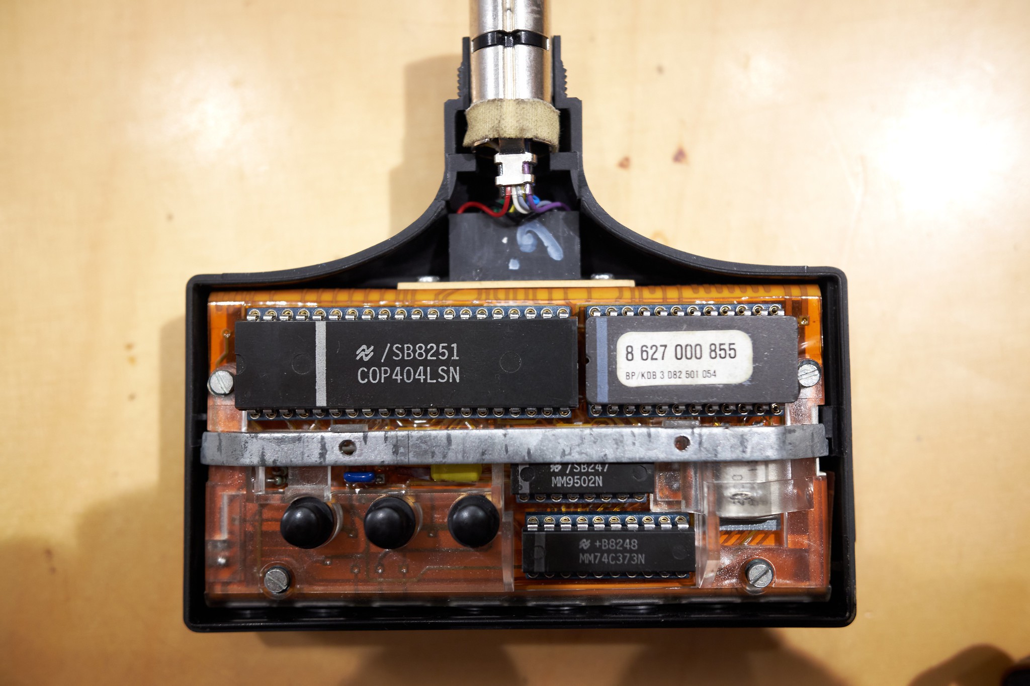
Apart from what you can see in the picture, the operator panel also contains an LCD display to output things like frequency and station name. It's all fitted on a flexible PCB. There are 22 input keys distributed over four of the six sides of the panel.
With all that user interface, It's no wonder that Blaupunkt needed a small computer in the panel to talk to the TMS9981 host CPU.
COP400 was a series of four bit processors originally designed by National Semiconductor for calculators. By the late 1970's, NS had three lines of processers: The COP400, the SC/MP and the IMP16. These were 4, 8, and 16 bit processors respectively. I happen to know the SC/MP very well as it was the CPU in my first computer. I had never worked with the COP400 though.
The COP400 series were mainly mask programmable devices with up to 2K of on-chip ROM. In the IQR 83, however, the code resides in an external EPROM. Good for us! We can have some fun looking at code!
Seeing the NS logo, I hoped the COP400 was similar to the SC/MP. While having its own quirks, the SC/MP instruction set was actually quite pretty. Studying the COP400 data sheet, I quickly realized the COP is much more strange! But let's look at the structure of the chip first to see what the instructions are controlling:
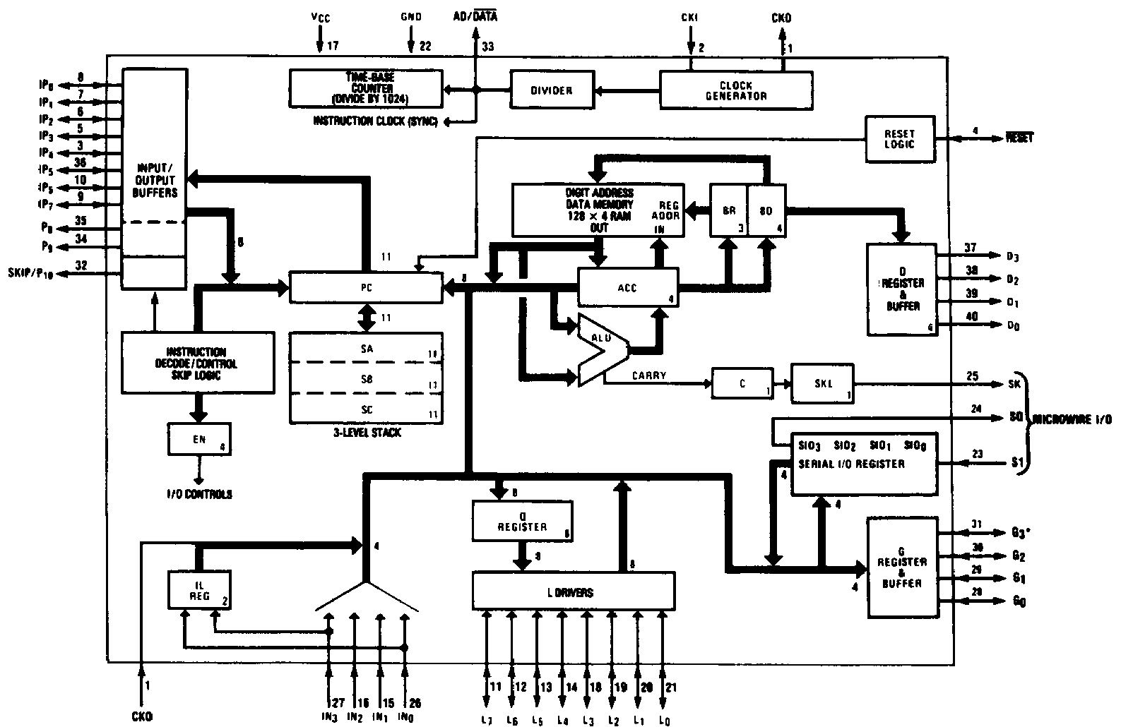
The block diagram above comes from the datasheet and shows the internal blocks of the COP404:
- I/O drivers and associated registers.
- Various registers: ACC, C, PC, Br and Bd-registers, and the three level stack.
- The 512 bit RAM block.
- The ALU.
- Supporting functions: Clock generator, reset logic, and the instruction decoder.
The interface to the code EPROM is via the IP lines on the left. Instructions are 8 bit and the least significant 8 bits of the address bus are multiplexed with the instruction bus in the COP404 (an external 74C373 latch decodes them).
The four bit ACC register is the source and destination for most I/O, arithmetic, logic, and data memory access operations. It can also be used to load input from registers. A 4 bit adder performs the artichmetic and logic functions. It outputs the carry bit to the one bit C register.
Data memory is 128x4 and organized in 8 'registers' of 16 'digits', four bit each. To access data in the RAM, the address of whatever needs to be accessed must first be set up in the two parts of the B-register: Br (register number) and Bd (digit number).
An unshown flag is the "SKIP" flag, which is internal to the instruction decoder: Many instructions have side effects setting that. When that happens, the following instruction is read, but not executed.
Let's look at sime simple code:
L110:	ININ		; Read Serial IN
	AISC	15      ; Add 15 to A setting carry...
	JP	$L111	; This jump is skipped if carry was set...
	JMP	$L110	; Continue reading until its a start bit
L111:   ...
This is jumped to after initialization and reads the serial port into the accumulator register. The AISC instruction is the "add immediate" instruction essentially adding a 4 bit number to the contents of the accumulator. But it has the side effect that if Carry becomes set, the following instruction is skipped.
This architecture may seem smart, but results in very convoluted and hard-to-read code. There are designated "TEST"-instructions that perform various tests on bit level or comparing the A register with a RAM location. These all set the skip-flag if the test is positive.
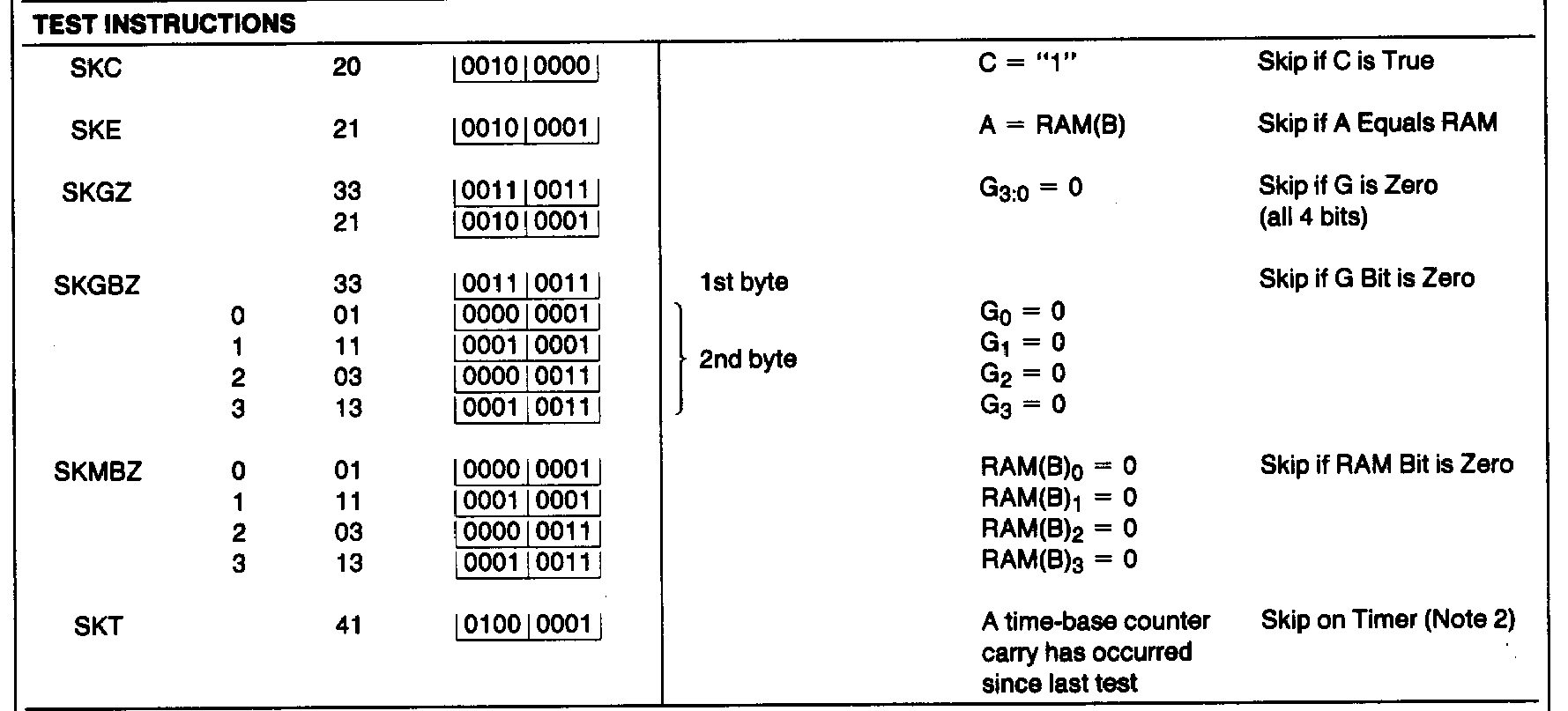 Another snippet from the initialization code, an example of one of the TEST instructions:
L1:	LBI	0, 0    ; B=0,0
	OBD             ; Output the Bd to the D outputs
	LBI	2, 9    ; B=2,9
	SKMBZ	0       ; If bit 0 of this RAM address is 0, skip next...
        JMP	$L117
The first LBI instruction sets the B-register to 0,0. Remember that the B-register is effectively the address register for the RAM, but in this case it's used for the value to output to the D port on the processor. The next LBI addresses RAM location 2,9, and if bit 0 of this is zero, it skips, otherwise it executet the following instruction.
I have uploaded a disassembly of the firmware, but I've stopped trying to reverse engineer the code as I realized it probably works fine as it is and I don't need to understand the internals to reverse engineer the interface. Much of the code, however, is just a software implementation of a 2400 baud UART.
Discussions
Become a Hackaday.io Member
Create an account to leave a comment. Already have an account? Log In.