 Michael Wessel
Please check out the Github for all future updates:
https://github.com/lambdamikel/picoram6116
A follow-up to my 2114 SRAM Emulator.
This time I am targeting the 6116 SRAM chip - full 2 KBs and a serious CPU at full speed (i.e., Z80 @ 1.8 MHz etc.)
Features
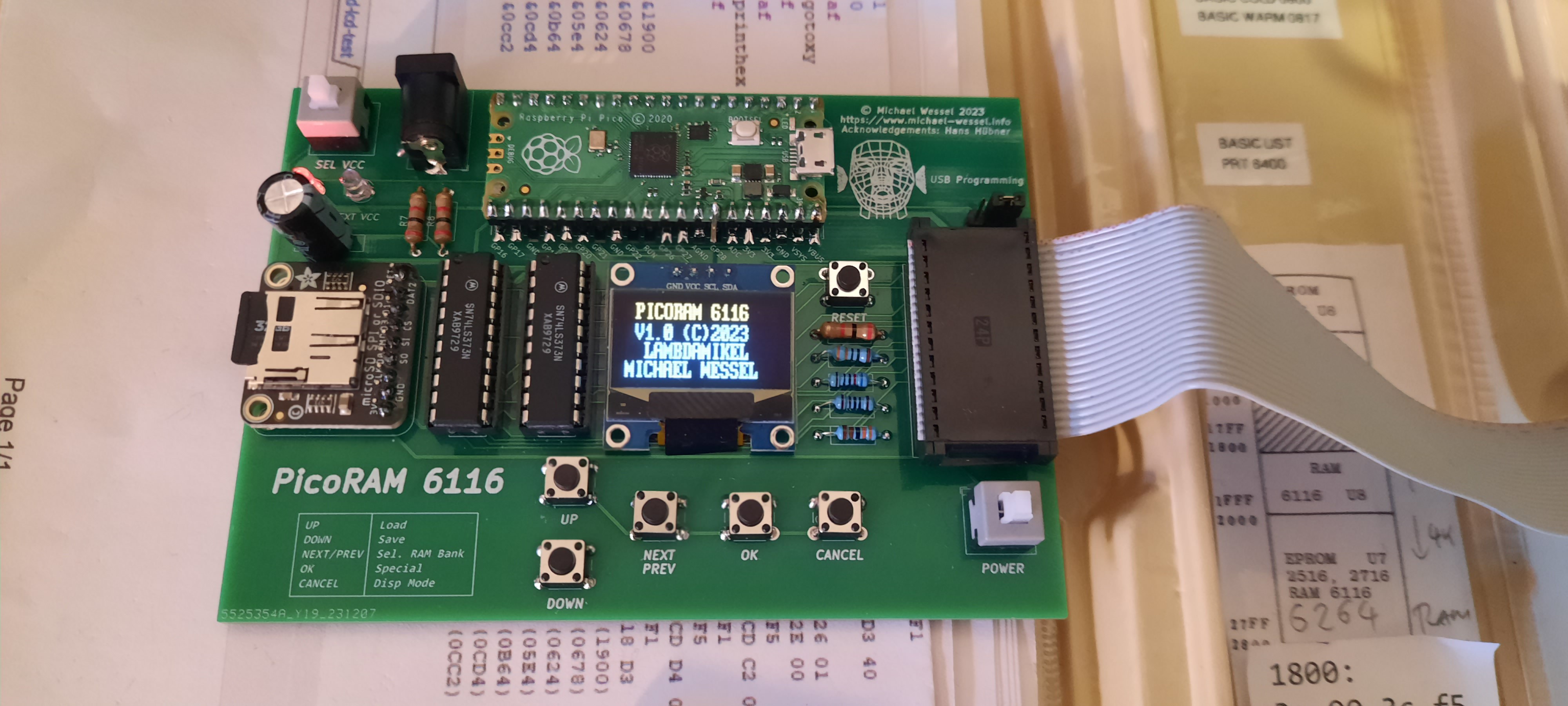
- Raspberry Pico-based SRAM 6116 emulation, fully software-based
- SD card for storing and loading of full 2KB memory dumps
- comfortable UI with OLED display for file operations
- ASCII HEX / FAT32 format facilitates file exchange and creation, e.g., with a PC assembler
- 4 user-selectable memory banks (UI buttons)
- powered directly over the 6116 power lines
- external power supply supported
- some nice LEDs
- versatile (i.e., should work with other 6116-based computers)


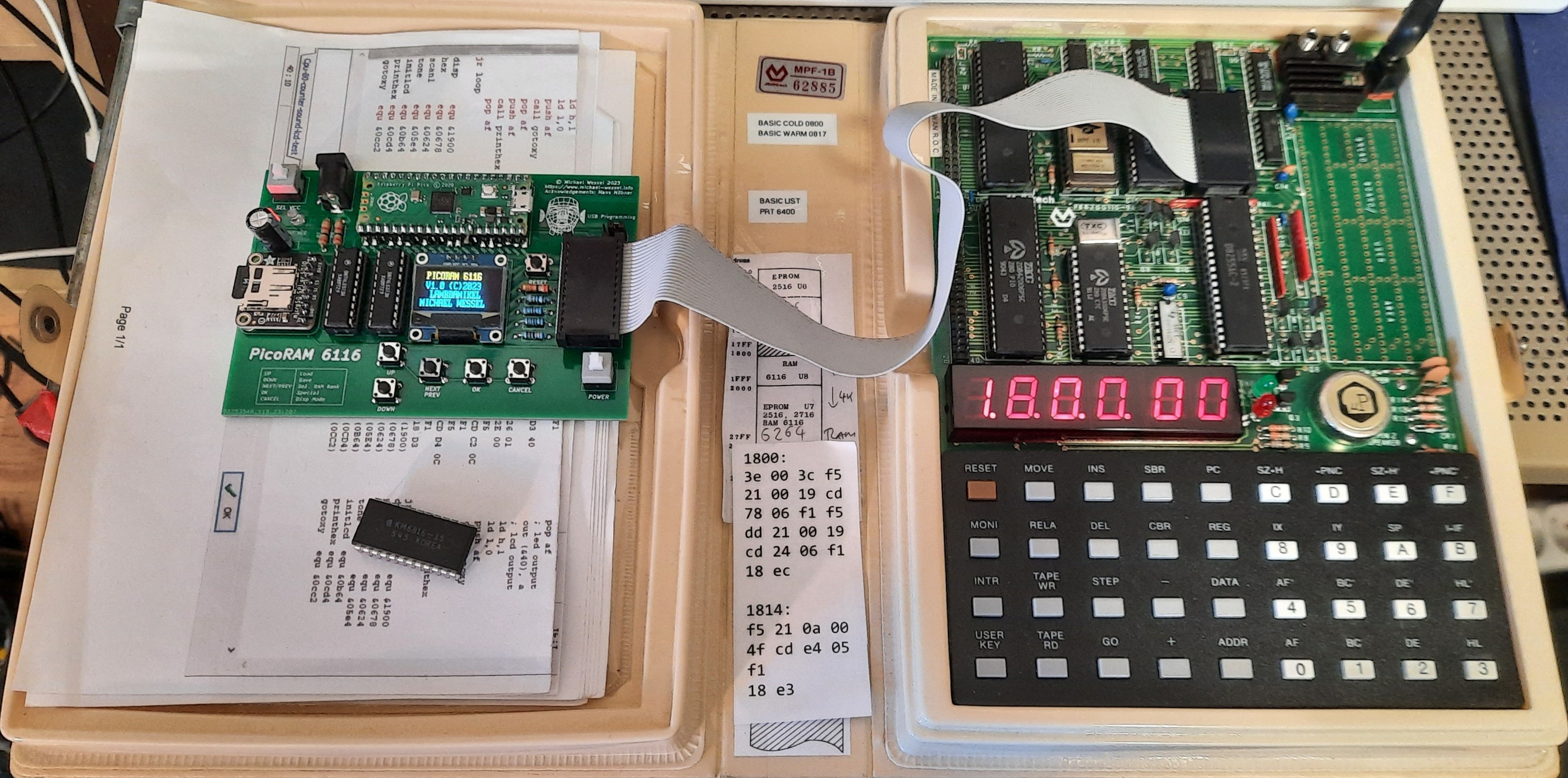
The Microprofessor MPF-1B is the first victim - it's 2 KB user & system RAM (U8) from 0x1800 - 0x1FFF is replaced by PicoRAM 6116:
Video:
The Microprofessor MPF-IP (One Plus, 1P) is the second victim - it's 2 KB user & system RAM (U5) from 0xF800 - 0xFFFF is replaced by PicoRAM 6116:

Video:
Theory of Operation
Well, this was a piece of work, and I wouldn't have succeeded without my trusted HP 1662A Logic Analyzer (see below for some details).
The first challenge was a lack of GPIO pins on the Pico. This wasn't a problem with my previous PicoRAM version, the 2114 emulator - the 2114 only required 10 address lines, 4 data lines, and a single WE (Write Enable) line. The Busch 2090 Microtronic which was the target platform for the emulator didn't even utilize the OE (Output Enable) line. In contrast, the 6116 now demanded a whooping 8 bits of data IO, 11 bits for the address bus, plus OE and WE - 21 GPIOs of the max. 26 that the Pico offers.
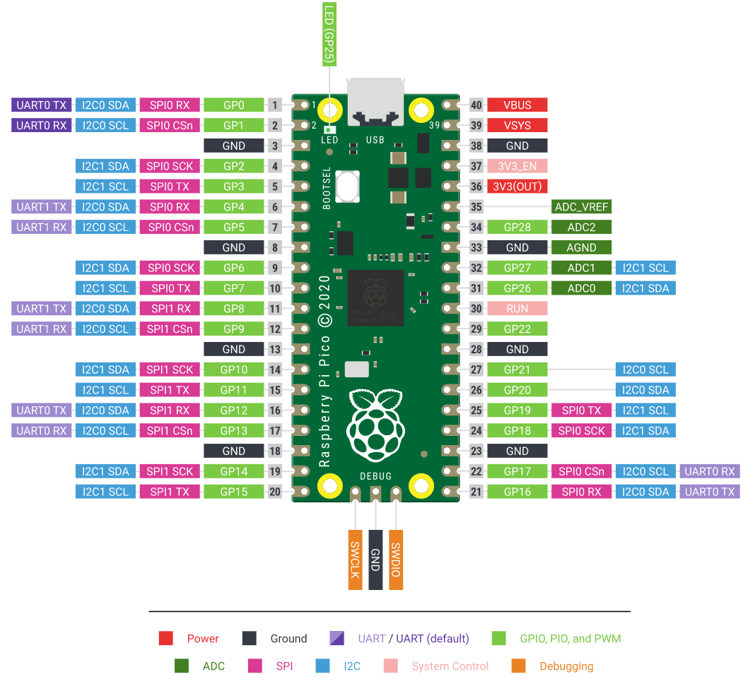
And, some of these had to be used for I2C and SPI, given that I wanted to keep the OLED display and SD card module. In addition, one analog pin for reading the 5 buttons. Hence, another 7 GPIOs became unavailable. I was hence short of by exactly 2 GPIOs to realize my dream design!
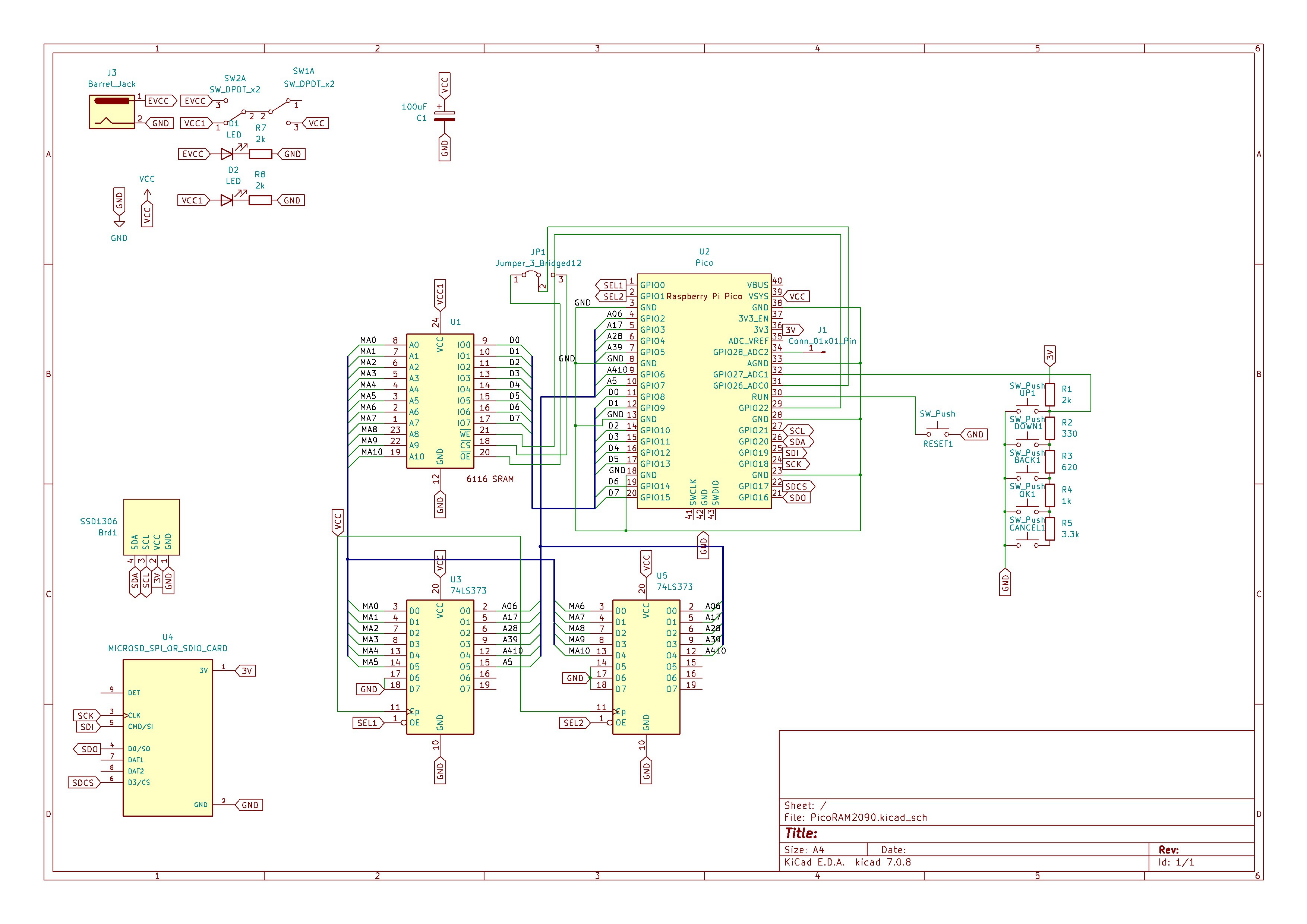
As a solution, I decided to multiplex the address bus - using 2x 74LS373 transparent 8bit latches, I came up with a design that introduced two multiplexing lines SEL1 and SEL2 to read the address in two batches - A0 to A5 in the first batch, and A6 to A10 in the second batch. The two latches are basically just used for their tri-state / High-Z ability; I am not even using them as latches. The LE is constantly kept high / 5V, making them transparent, i.e., any change to their inputs is immediately mirrored to the outputs, if enabled (their OEs are connected to SEL1 and SEL2, respectively).
Using this design, I now even had one spare GPIO left! I still don't have any good idea what to do with it, so it's just left as an open pin on the final version of the PCB (the extra pin is not shown in the video yet). Maybe for sound output. It was already extremely useful for analyzing the Pico's timing, i.e., determining the exact execution time of a piece of firmware code in nanoseconds (-> HP Logic Analyzer).
Please note that, unlike my previous PicoRAM 2090 2114 SRAM emulator, I did not include any level shifters or resistors networks. This Hackaday article, and my practical experience with PicoRAM 2090 running for hours without damage without voltage level conversion, convinced me that the Pico / RP2040 really is 5V tolerant. So I am not expecting any issues from that.
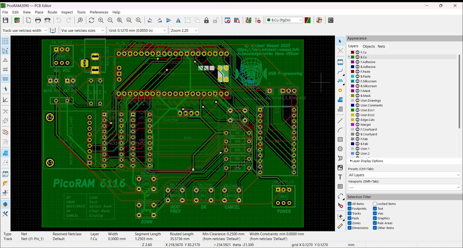
After a number of iterations, the final PCB looks like this - I have to confess that I needed 4 iterations this time. The availability of very inexpensive PCB production services in the far east made me definitely a bit more careless and more daring in that regard compared to previous projects. Also, I didn't do a breadboard prototype this time... my 3rd iteration PCB (seen in the demo video above) still has a glitch that requires a bodge wire - I forgot to connect LE to VCC...

This is the final version:
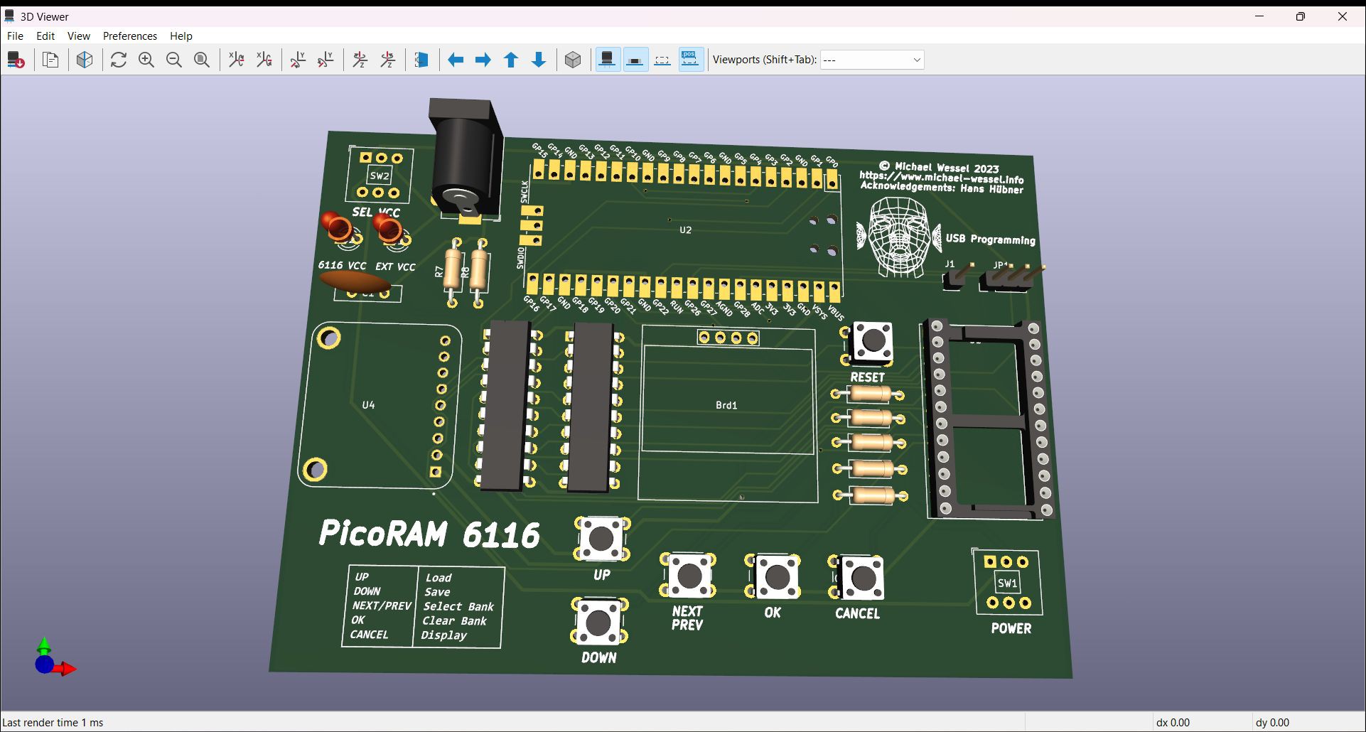
The MPF-1B video shows Rev. 3 which stil requires the bodge wire, and the MPF-IP (1P) video the final version of the PCB.
Pulling Down WAIT
The spare GPIO is by now used for pulling down the Z80's WAIT line while operating PicoRAM UI (i.e., replacing the RAM contents, clearing or swapping banks), That way I also no longer need to hold the machine in RESET while booting or powercycling. You can see the WAIT bodge wire in the MPF-IP video.
Getting the Timing Right
With a project like this it's all about getting the timing right. I first tried to "blindly" write code that would do "the right thing", and make this as fast as I possibly could. Basically, the emulator is running a number of very tight busy waiting loops - wait for CE to go down, then read the address, then check if WE goes down, then switch the GPIO direction for the data bus from input to output if required, etc. However, timing is really critical, and I wasn't sure how critical. For example, should we first wait for the falling edge of CE and then read the address, and at what time after (or even before?) the falling edge of CE is the address bus stable? And same questions for the data bus - how long should we wait after the falling edge of WE to read from the data bus, when is it stable? Etc. Obviously, there a lot of variables, and if the timing is even slightly off, then the whole thing just won't work at all.
I quickly realized that doing it blindly via "trial and error" wouldn't result in a solution soon. Just too many unknowns and variables. First, I needed to learn exactly how the timing of the 6116 works. Next, I also needed to understand how much time certain pieces of code take when executed on the Pico. I have overclocked it slightly to ~ 260 MHz to have some more slack. I am a proud owner of a gorgeous vintage HP 6162A Logic Analyzer with more channels than I could every use (68!). So I hooked it up to CS and WE (after realizing that OE is not being utilized by the Microprofessor MPF-1B), A0 and IO0, and then analyzed the timings.
I found that the WE and CS pulse widths are 1.120 us, which is a relieve as it gives us plenty of time to work with - for example, reading the address bus by demuxing the 2 74LS373 takes about 260 ns, so after all, it seems that this was going to be feasible! I also found that there are about 480 ns between the falling edge of CS to the falling edge of WE in case of a write operation, and about 0 to 80 ns between the rising edge of WE and CS (occurs almost simultaneously). We have about 160 ns between the falling edge of WE before the data input is valid. Moreover, it turns out that the address is stable long before the falling edge of CS - 320 ns before!
Here is a typical Logic Analyzer screenshot, showing a write operation - from top to bottom: WE, CS, A0, and IO0. The relevant transition of A0 (rising edge) isn't visible, as it occurred way before the falling edge of CS (out of screen area, on the left):
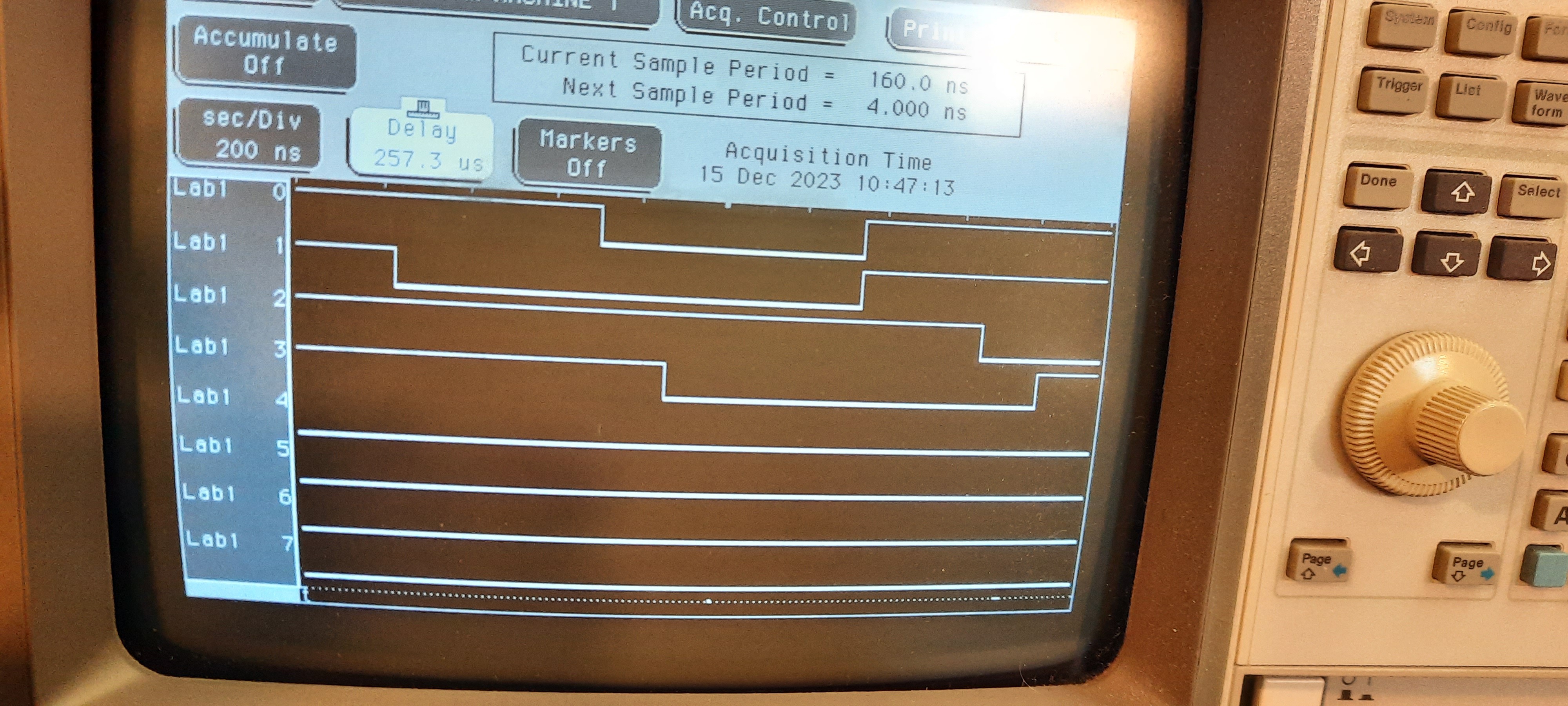

By also measuring the execution times of the various tight loop contents and conditions, I was then able to arrange the code in such a way that all the operations occur within valid time frames. The extra unused GPIO pin was turned into a "signal" pin - by toggling the pin on and off and observing these transition vie the Logic Analyzer, I got a good understanding of exactly how long certain operations take.
Finally, after some back and forth and rearranging of code, loops and conditions, and shuffling read and write operations around to the right positions, I was able to get a faithful emulation of the 6116. It wasn't easy though, and definitely not possible without a Logic Analyzer. I guess it took me about ~10 hours to implement just this part of the project.