 mihai.cuciuc
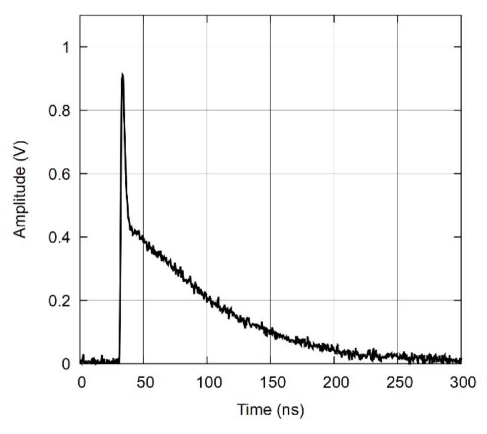
SiPM pulses have fairly large amplitudes so don’t need a lot of amplification, but they have fast rise-times below a few ns and decay times in the range of hundreds of ns. The figure below is an example pulse provided in the Broadcom AFBR-S4N44P014M datasheet.
The easiest way to digitize its amplitude with a slow ADC would be using a very fast peak detector that can handle the high frequency content of the rising edge. But this wouldn’t be very low power as the peak detector has to be constantly enabled to catch pulses, and fast op-amps draw high current. My approach is to “round off” the pulses using RC integrators to slow them down, and then triggering on this slow version of the pulse to enable a peak detector before this pulse reaches its maximum. While this sounds easy, it was my first attempt at some analog design so I ended up spending a few days simulating it in PSpice for TI. This is the schematic I ended up with in the simulation, with components grouped into functional blocks that are described below.
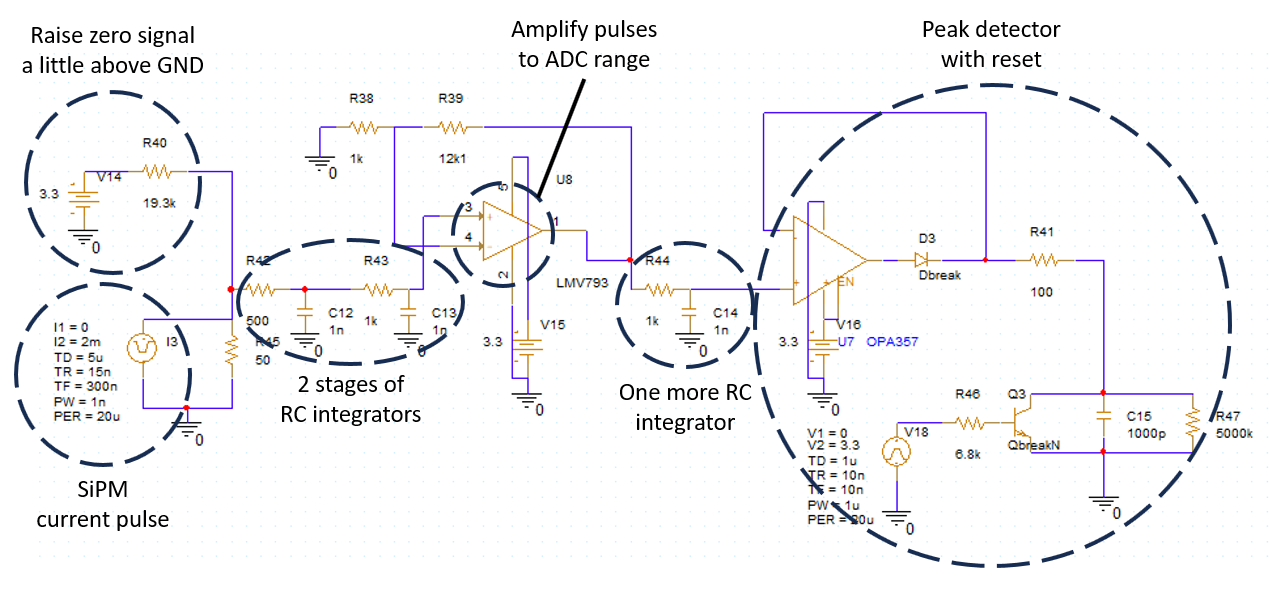
SiPM
I simulate the SiPM as a current source that produces a pulse with a shape that approximates what I measured on the oscilloscope. The limited bandwidth of my measurement setup made the rising edge less steep so I generate a pulse with a 15ns rise time and 300ns fall time. The current amplitude is chosen to provide some hundreds of millivolts on a 50 Ohm resistor.
Raise zero signal a little above GND
This is just a resistor from 3.3V to inject a small DC offset into the measurement. The op-amp outputs in the system don’t go down to 0V, but have a minimum output voltage of 100mV or so. So this is a very simple solution to cope with that. It does cost a little though – the ADC input DOES go to 0V, so I lose a little bit of ADC range.
2 stages of RC integrators and another stage after the first op-amp
These round off the sharp input pulse to much slower pulses. There are two tradeoffs though. One is that you lose amplitude, but you can easily recover that using subsequent amplification stages. The second tradeoff is that in high count-rate applications you can get pulse pile-up, where the detector provides another short current pulse before the integrator output reached down to zero -- and that makes your measurement wrong. Serious analog processing uses a series of CR differentiators and RC integrators together with pole-zero compensation networks to create nearly gaussian pulses.
Amplify pulses to ADC range
The LMV793 is a decompensated op-amp. This means it’s much faster than op-amps with similar power requirements, but it’s not unity-gain stable. It only works at high amplification, in the LMV793’s case more than 10x. This is the only place in the circuit that allows for some flexibility in setting the gain, apart from the bias voltage on the SiPM. Thus this gain is set to match the gamma spectrum range to the ADC range. As this op-amp needs to be constantly powered it will significantly contribute to the total system power draw -- the LMV793 is spec'd to draw at most 1.65mA so it should fit in my power budget.
Peak detector with reset
This is just half of the peak detector circuit. Another unity gain buffer follows, but for this simulation it’s unnecessary. The 100 Ohm series resistor is there to make the op-amp happy driving a capacitive load. The OPA357 has an enable input (not used in this schematic) that can turn the op-amp on in 100ns. So as long as the trigger pulse is generated well in advance the peak detector should consume no power until it’s actually needed. And then after reading the stored value it can be shut down until the next pulse. This section of the simulation also contains a pulsed source that periodically resets the peak detector such that I can simulate several pulses.
Most peak detector designs use identical op-amps for both the ideal diode as well as the unity gain buffer (that is not included in this schematic). This allows those designs to use fancier feedback loops that minimize capacitor discharge or improve response to short peaks. However I decided to keep the loop simple because I was afraid of circuit behaviour when enabling both op-amps and then expecting a valid result in a few hundred ns. Keeping separate feedback loops for the ideal diode and the voltage follower allows one to treat them independently. Additionally the voltage follower can now be a much slower op-amp that even when active will draw very little power contributing a little to making a low power design. I decided for a TLR341G for this.
I used two great resources for understanding what I'm doing while designing this section:
EEVblog's video on peak detector circuits
Section 4.5.1 from The Art of Electronics, 3rd Edition
PSpice for TI simulation
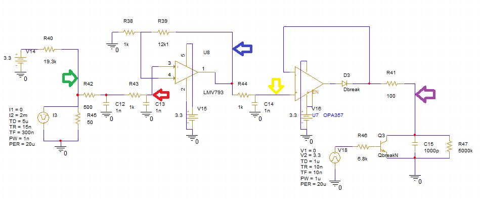
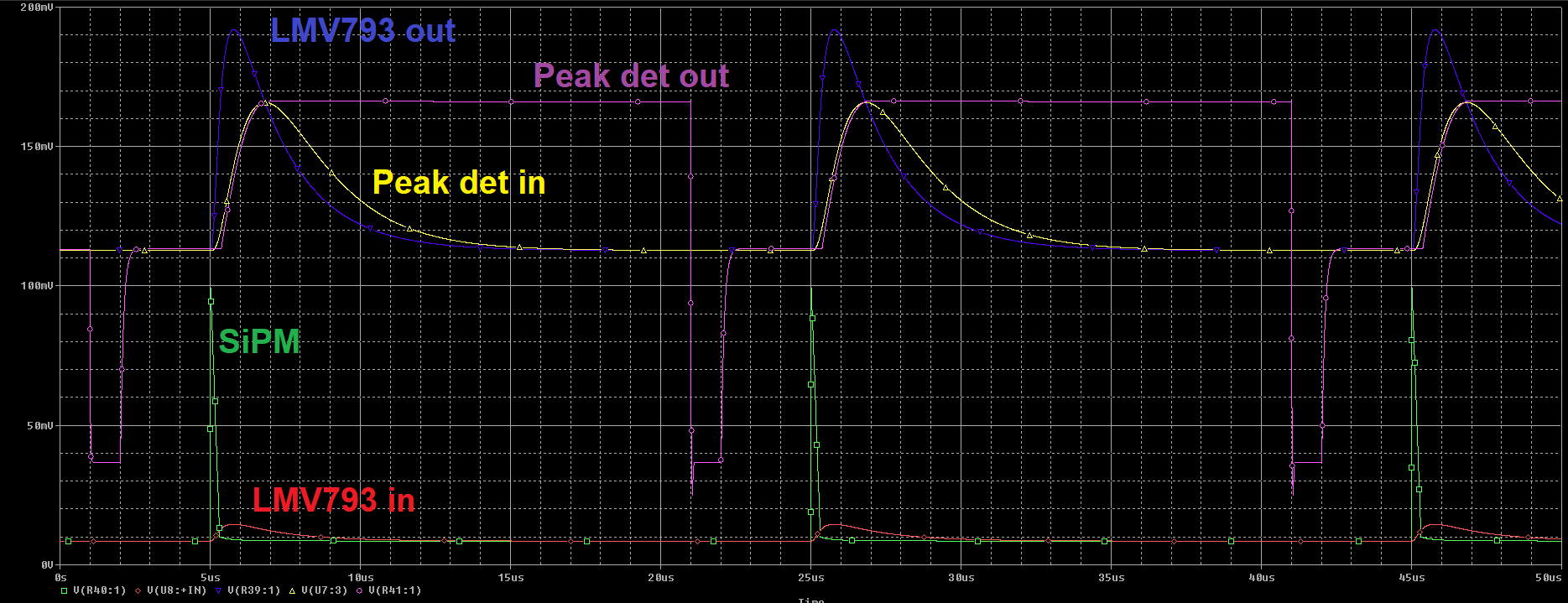
To validate all of this I ran some simulations with different pulse amplitudes to confirm the system behaves linearly. Below is the schematic with the color-coded probe points, as well as the simulation results.
Conclusions
Not included in this simulation is the trigger section. A comparator triggers on the LMV793 output and enables the peak detector. Simulations shows that there are several hundred ns between the LMV793 output rising above a set threshold and the peak detector input reaching its maximum, thanks to the additional RC integrator in between the two. So this whole thing should work.
These integrators do pose a limit on how closely spaced pulses can be. One can see the peak detector input returns to baseline in ~15us so this will not properly handle very high count rates. I expect ~20 kCPS (to account for statistical fluctuations) should be doable without messing up the energy resolution.
Discussions
Become a Hackaday.io Member
Create an account to leave a comment. Already have an account? Log In.