 mihai.cuciuc
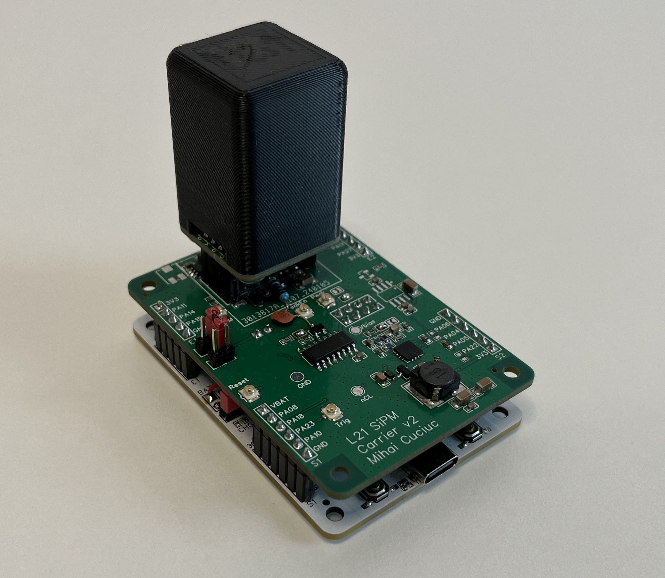
I integrated the analog front-end and the MAX1932 power supply into one single plug-in analog board that the detector can then be plugged into. I used this together with the 10mm x 10mm x 30mm CsI(Tl) crystal to form a system with the following performances:
- Energy resolution @ 662 keV: less than 9.5%
- Current draw @ 12CPS: 6.5mA
- Current draw @ 2300CPS: 7.7mA
Analog front-end
This is the circuit simulated in the Analog Front End log entry. It has two RC stages, a fast decompensated op-amp with low current requirements, another RC stage, and then it goes to the peak detector. The first op-amp of the peak detector is an OPA357 that draws quite a lot of current. The second one, a voltage follower, is a low power part, as it can take all the time in the world until the ADC is ready to digitize the signal. To save power, the peak detector op-amps are only enabled when there’s a signal to be measured, thus saving a lot of power. The OPA357 needs to respond very quickly to an incoming enable signal, and the datasheet provides a turn-on time of 100ns. PSpice for TI simulations showed that there are several hundred ns available.
Trigger
The threshold for measurement is set by the MCU through its DAC, setting the minimum pulse amplitude to trigger a measurement. A fast, low-power comparator (TLV3201) supplies this trigger signal that gets sent to the peak detector op-amps enable pins to switch them on, and also to the MCU to wake it up and start a measurement. To keep the peak detector active for as long as needed by the MCU, the trigger signal goes through an S/R latch that is only reset by software. As the low-power S/R latch used (MC14043) quotes propagation delays as long as 350ns at 5V, there is a fast bypass for this signal with a diode-OR between the latch output and the incoming trigger signal.
Validating the simulations
The board has multiple analog test points that make it easy to trace the functionality of the device and check against PSpice for TI simulations, with an example in the figure below.
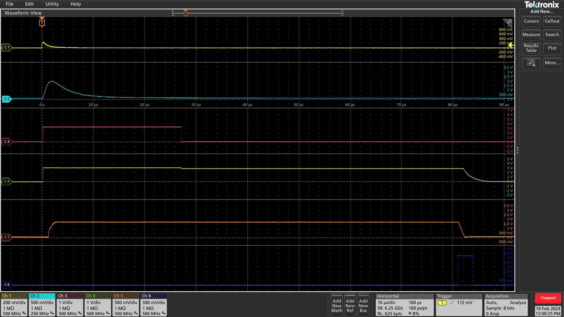
Ch1: SiPM output
Ch2: Shaper output. It is sent directly to trigger comparator. It goes through another RC filter before being sent to the peak detector
Ch3: Trigger comparator output
Ch4: Peak detector enable. This is diode-ORed between trigger comparator output and the output of an S/R latch that is set by the trigger comparator. This ensures fast propagation of the signal to enable the peak detector (S/R latch propagation delay is several hundred ns) and also that the peak detector won’t switch off unless told so by software
Ch5: Peak detector output. This signal goes to ADC
Ch6: Peak detector reset. This signal clears the peak detector capacitor. While it’s set the peak detector is also disabled through the S/R latch.
The entire measurement takes ~85us, but I tracked some of the time spent in the interrupt handler mechanism which has to check every external interrupt line. I could hack a way around this to bring the measurement to ~45us.
Discussions
Become a Hackaday.io Member
Create an account to leave a comment. Already have an account? Log In.