 Keith
Keith2024-01-20
I've just found and bought this board from eBay. Made by DSP Design Ltd.
It uses the 7-thou pitch DIL packaged device (ugh!) which can only access half the memory of the PLCC68 version.
I don't expect this to come with a manual or circuit diagram, so some reverse-engineering is expected.
I bought this to have a look at the circuit and the firmware ROM. Maybe I can port a ROM-based CP/M onto it.
2024-01-24
It is now in Istanbul, Turkey. 36% of the way here. At this rate it will take a week to arrive.
2024-01-25
Now in Bury St. Edmunds.
2024-01-26 13:06
Arrived! Took some quick pics. Sorry about the flash glare, I'll take some in daylight tomorrow.
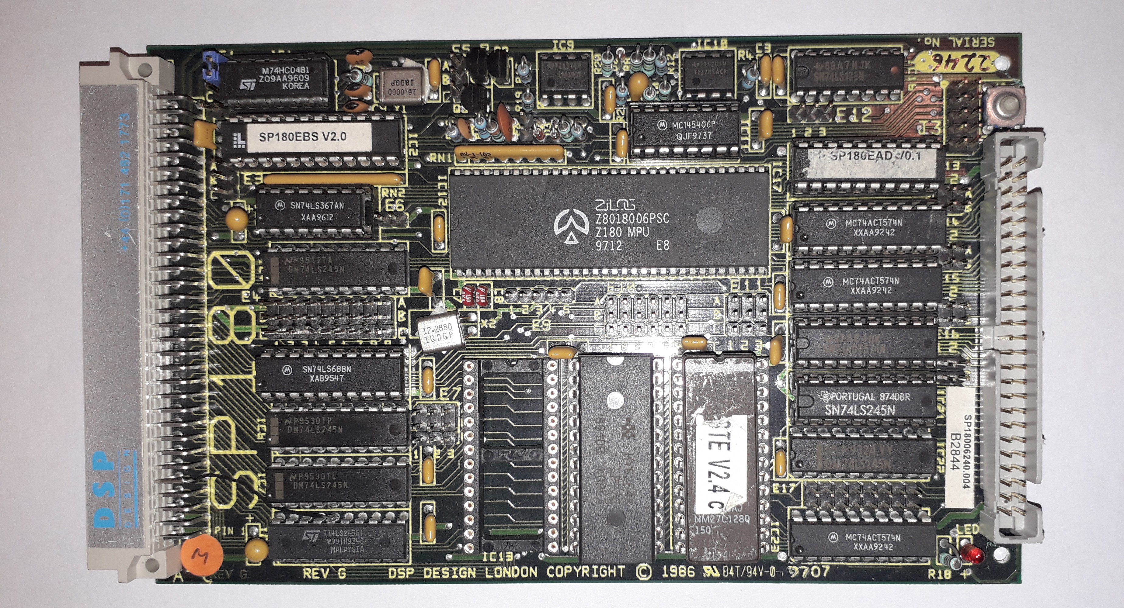
The top side shows
- It has three 8-bit buffer and three 8-bit output latches.
- The two crystals (16 and 12.288 MHz) are an unusual miniature size
- One ROM socket with one 16k EPROM
- Two RAM sockets with one 8K SRAM
- Z180 processor is rated 6.144 MHz
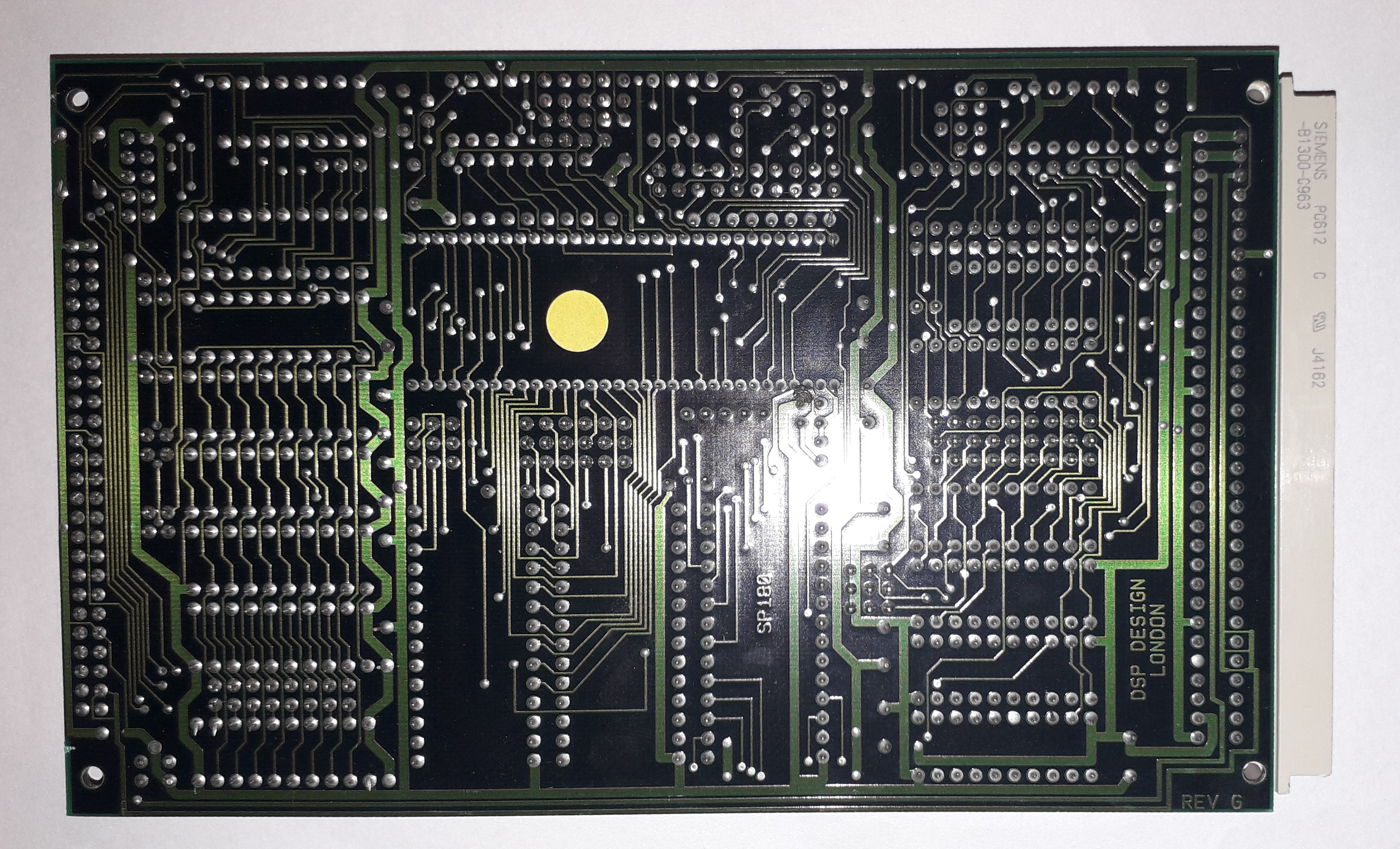
The underside is very dark so this is probably a 4-layer board which will have made it more expensive.
Parts list
IC1      74HC04B1 forms the 16 MHz oscillator circuit
IC2      Lattice GAL22V10-15LP with program SP180EBS version 2.0
IC3      74LS367AN six-bit buffer
IC4,6,7,8  74LS245N eight-bit buffer
IC5      74LS688N eight-bit comparator
IC9      LM393P
IC10     TL7705 reset circuit
IC11     MC145406P is an RS232 buffer
IC12     Z8118006PSC (Z180, DIP64, 6.144 MHz rated)
IC13,14  RAM sockets, DIP28
IC15     ROM sockets, DIP28. Software is STE V2.4c
IC16     74LS138 one-of-eight decoder
IC17     Lattice GAL16V8B-25LP with program SP180EAD version 0.1
IC18,19,20,23  74LS574 eight-bit output latches
IC21,22   74LS245 eight-bit input buffers
C6,C7,R1  part of the 16 MHz oscillator
C7,8      bias the 12.288 MHz oscillator circuit
The date codes show that the CPU was made 11 years after the board was designed, indicating an impressive product design life span.
Initial investigation
IC17 (a GAL16V8) senses A18...A15 and can then decode the 512K address space to 32K boundaries. This is a convenient size, matching popular RAM chips and filling half a Z80 memory map.
IC2 (a GAL22V10) is the STEbus interface.
I removed and read the EPROM successfully. I expected the GAL chips to have their security bits blown, but they were not, so I read those as well.
More track buzzing suggests that this is a slave board, not a master! It would explain the LS688 address decoder chip. It looks like the STEbus can request the Z180 bus, access the memory as a 4K block, then release it back to the Z180.
This is a bit disappointing, I already have a slave Z180 board (albeit non-responsive) and I wanted a bus master board. However, it avoids the need for talking through a back-to-back latch (74LS645) or a dual-port memory (Zilog FIFO in DIP40 package).
As you can see, the PCB is mostly occupied by the three memory chips, the CPU, and the bus buffers. There is very little room for the parallel I/O chips at the front of the board. A modern design would use a micro controller instead.
A web search suggests that that their bus master was called the SX180.
I believe the board was never used, because there were no links for setting the memory types. I have now set them for 16K EPROM and 8K RAM.
Discussions
Become a Hackaday.io Member
Create an account to leave a comment. Already have an account? Log In.