 MS-Dzo
Hello everyone, i've been hard at work ̶g̶e̶t̶t̶i̶n̶g̶ ̶m̶y̶ ̶c̶a̶d̶e̶n̶c̶e̶ ̶l̶i̶c̶e̶n̶s̶e̶ ̶b̶a̶c̶k̶ on the DAC, but also "redrawing" the whole project.
First things first, let's address a few important points/thoughts I had since last time :
- What will the Output Unit (DAC unit / DAC / Power amp) topology be like.
- Changing the mixing algorithm
- I2S means Inter-IC Sound, so how can i make a modular system (ie : multiple PCB for multiple inputs/outputs) since length of track will be variable ?
- the choice of ICs need to be done so I can start designing the circuit.
- How do I test this.
Let's see those points in detail.
1 - Output Unit structure details / Amplifier talk.
One thing that might have not been clear before is that the mixing unit acts as a separation between the sound sources and the amps/headphones/whatever : Any data out of the mixer either goes back to the sources through USB (as a microphone input) or get sent out through I2S. What we're currently designing is the "DAC", or the output unit, used to transform the I2S into analog signals that can then get amplified by any kind of analog amp.
Analog amplifiers come into a really wide range of configuration, each with their own unique ups and downs. Class A, B etc. are easy enough to make but are rather inefficient, while class D amps are the opposite : really complex, really fiddly, really efficient. Making a class D amp entirely by myself is out of the question, but chips do exist that allow for the dreaded analog to 1 bit modulation. Most class D amps out there are made with ICs taking analog in and spitting HF PWM out that get filtered back to ~20Hz - 20kHz.
The idea is therefore to create a "comparator amplifier" that acts as closely as possible as an ideal opamp in comparator mode : taking the HF PWM signal (with "Voltage High" and "Voltage Low") and spitting out a symetrical Signal (±V amplifier) such that both waveform are exactly the same, just with different amplitudes.
Here's the structure of the output unit with power amplifier attached.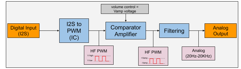
As you can see, volume control is entirely determined by the power supply of the entire output stage.
In our case, the output unit actually needs at least 2 analog output : Line Out and Headphones Out. I'll just do the same comparator Amplifier + Filtering Combo on the same PWM input to get both signals, with different V_amp voltages for each.
I'll also allow a PWM output because my portable DAC unit won't have a beefy variable voltage source needed for the power amplifier part. Therefore, i want to future proof it by being able to be connected to such an amp down the line : making different modules make prototyping much easier.
NB : by choosing this method, i completely bypass the analog pre amplifier needed for the input module that i was supposed to design now, which mean i'll have to design it later.
NB : This output module is entirely optional, there exist many I2S to Analog DACs out there. I'm just designing it because it's fun.
NB : This method moves the complexity away from the actual amplifier design and toward the power supply design.
2 - Sound with 32 bit-depth makes no sense
In the introduction of the project, I devised a few ways to deal with potential overflow. Since i wanted to not deal with distortion so much, i decided to just put the 24 bits + overflow onto a 32 bit channel and pretend everything was fine. it's not fine.
So, let's say we have a 32 bit DAC chip, working with a specific voltage. It takes I2S as an input and output an analog signal using what is black magic for our intents and purposes. That output should be perfectly linear. Well, let's say we're using a symmetrical 5V power supply. The DAC's resolution is 10/(2^32) volts, or roughly 2.33 nanovolts. Let's be clear, that's absolutely impossible to achieve, which means the least significant bits of our signal are straight up noise. The DACs are more expensive, I2S timings are tighter, everything is more complex... it doesn't help at all.
So, i'll have to find a way to stay with 24 bits. Luckily, i'm still a student ! I asked one of my professors and he dropped a few truth bombs on my algorithm, mainly :
- Audio sources are not correlated, so the chance of overflowing aren't that great
- Even if overflowing happens, it's not the job of the mixer to deal with it. rather, there should be variable gain higher up the chain.
- As such, the true ,final algorithm™ should just be an addition.
Hell yeah, look at me winging it as i go.
3 - How do I send the I2S far far away ?
for 24 bit 96kHz, we're looking at a ~2.3Mhz signal. That's doable, but the issue comes with the specific rise/fall times needed. Long story short, it depends on what IC I end up using but overall length of the track remains an issue.
I've found a few ways to deal with it :
- Bringing the modules really close to the mixing unit (like addons directly on the main PCB), and just sending the control/PWM/analog signals to and from the rack mounted "face plate".
- Making the I2S a balanced signal that gets unbalanced at each end of the wire
- Using buffers (comparators really) to deal with the rise/fall times.
All of those (or a mix of them) should solve that issue, I haven't really thought about it much yet because i'd rather start designing the actual standalone DAC unit first.
4 - general IC choices
I've previously highlighted the structure I've chosen for the output unit in part 1 of this post, but all the actual hardware choices aren't made yet.
Let's recap on what our bridge specs are :
- The USB bridge MUST be duplex (USB device acts as audio input, and audio output).
- The USB bridge MUST be an USB slave
- The I2S lanes MUST be stereo, turning mono to stereo by copying one channel to the other if necessary.
- The I2S/USB lanes MUST be 24bit 96KHz.
- The I2S lines MUST be controlled by the FPGA (not the microcontroller itself). That means that buffering USB data must be done, so that the bridge and the FPGA can be synchronous.
→ The duplex 24bit 96KHz audio spec means that we'll have to deal with USB Audio 2.0 class.
→The duplex I2S lines means that we'll have to use a microcontroller with two internal I2S processors
Let's recap on what our DAC specs are :
- I2S Input (24bit 96kHz)
- PWM Output
- Cheap
- Currently produced
- Share the supply voltage with the microcontroller.
That's it. I know the THD will be correct either way so i'm not even asking for specific values.
→ Choosing the DAC chip first, i've found the TAS5548. It does everything i want.
The chip isn't a DAC but a PWM modulator, as we've talked about earlier. It needs to be driven by a microcontroller to initialize it, and i'll use the Bridge IC to do so.
→ For the Bridge / Output controller, i'll use a cheap STM32 with one USB interface and two I2S ones.
The choice of a STM32 is pretty inconsequential. I'm simply used to the dev environment.
Chances are, the input module will also have a few parts to be initialized (the ADC for instance).
There's also the fact that the face panel of the Input or Output modules might act as rather complex HID devices depending on how much feature creep and rule of cool engineering i want to deal with. ( mute buttons, motorized potentiometers etc.).
If that's the case, having a bridge chip with processing power to spare might prove useful. In any case, price is key and the I2S to USB / USB to I2S pipeline seems pretty straight forward.
5 - Testing setup
Measuring is a critical step to know wether or not the system actually works, but measuring binary strings is a gigantic pain, yet I have to insure that my USB bridge works.
One quick way to know at a glance is to play a sound file on my computer and listen to what the DAC spits out, but that's obviously not enough.
Here's the plan :
I'll make a test audio file with specific values and play it on repeat. Then, i will measure what the bridge spits out over time, and see if those hex values correlate to what is expected.
Once we have a working bridge, we can go lower down the chain and connect it to our DAC. We should then be able to measure the frequency response of our system against the original audio through a digital signal generator, which should give us a clue on how linear we are (ideally we'd want 0dB)
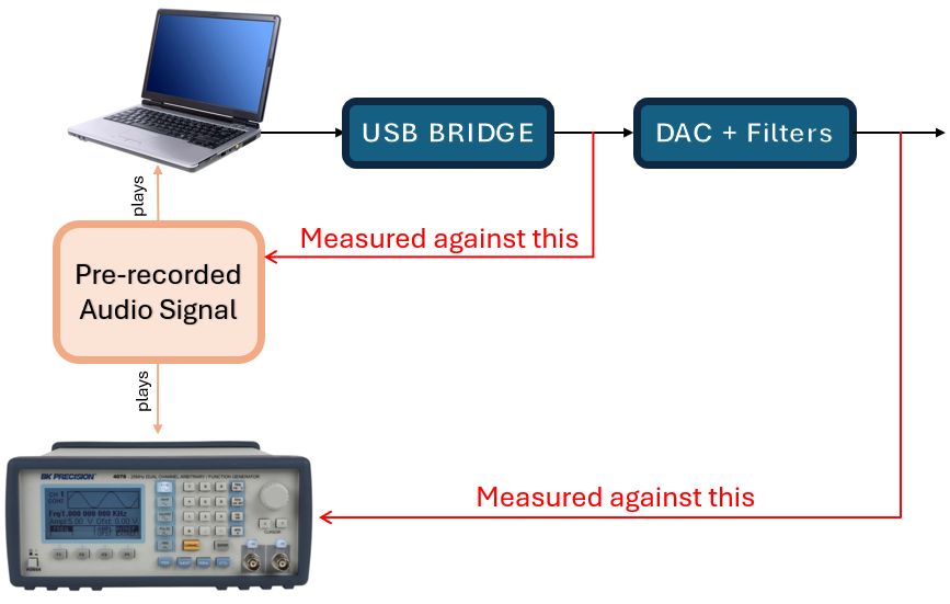
Once we reach that point, we have a working USB Bridge and DAC. Can't wait !
Just a small word for the end, I'm sorry for the lack of actual content in these posts. I'm still actively studying, looking for overseas internship and whatnot so that doesn't leave a lot of time for leisure work. I also have a big case of no money so buying PCBs and chips is difficult to say the least. If you have any question or would like to work on that project, please don't hesitate ! it'd be fun to work together :)
Anyway, next blog post should be about routing and filtering. Cya !
Discussions
Become a Hackaday.io Member
Create an account to leave a comment. Already have an account? Log In.