 teardownit
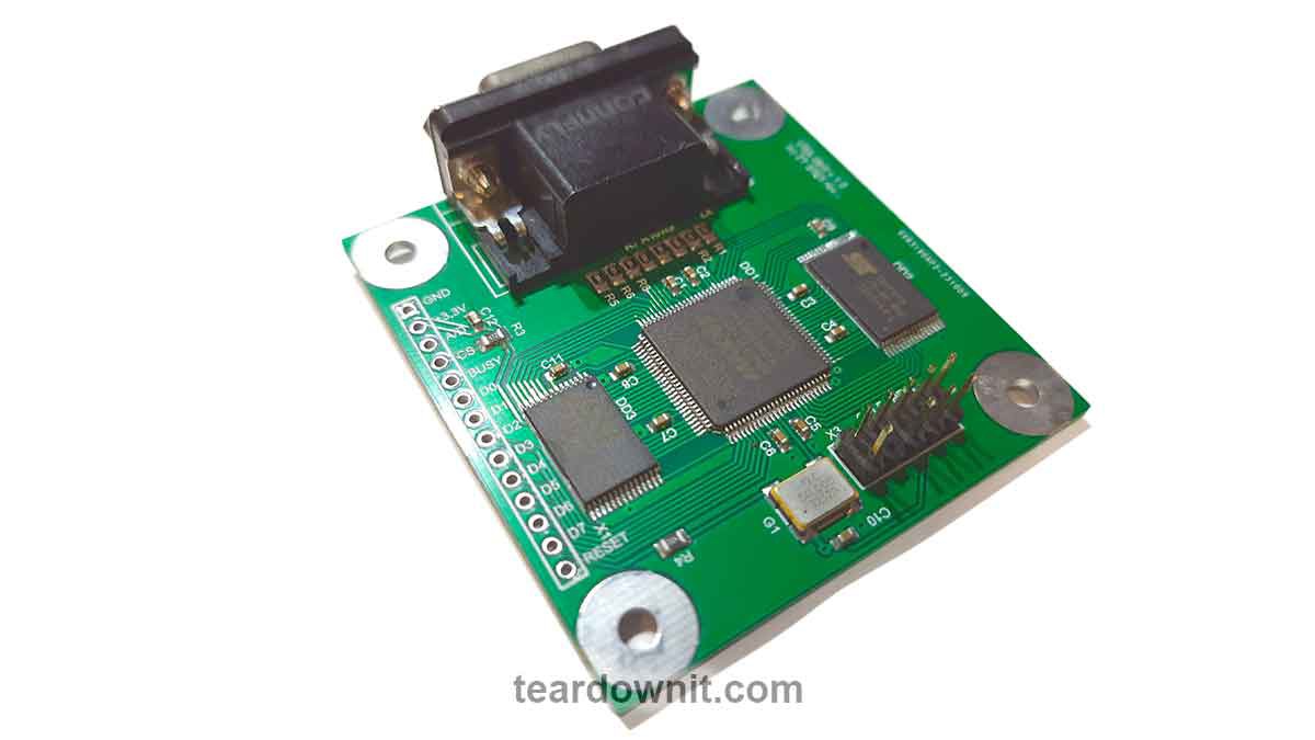
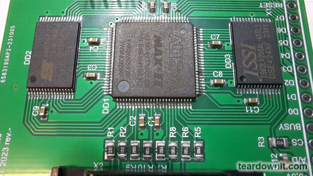
First of all, you should pay attention to the ROM used. The flash-ROM chip from an old computer motherboard has a finicky parallel interface where the address is written in two runs. This complicates the operating logic and increases access time. Additionally, the PLCC housing it comes in can be expensive and challenging to install manually. In this regard, it was decided to replace it with a more modern 39-series microchip from SST. These chips, such as the SST39LF and SST39VF, have faster access times (55 ns and 70 ns, respectively) compared to 270 ns for the 49 series chip. This allows one to reduce data preparation time to one cycle. The SST39VF010-70-4C-WHE chip has been ordered.
It is also necessary to replace the RAM. To save money, I picked one that operates precisely at 3.3 V and has TSOP housing. The IS62LV256AL-45TLI chip was ordered.
The CPLD chip remains unchanged.
These updates improve overall efficiency by reducing memory access times and using more convenient and modern components, which can also improve product availability and reliability in the future.
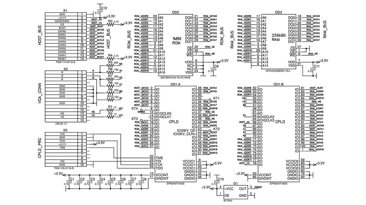
The updated diagram is shown below:
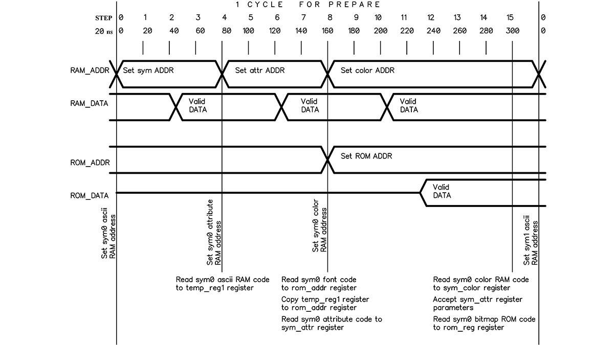
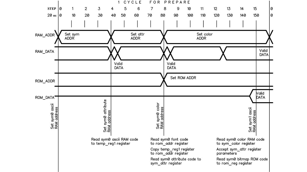
The timing diagram for new chips has become much more straightforward:
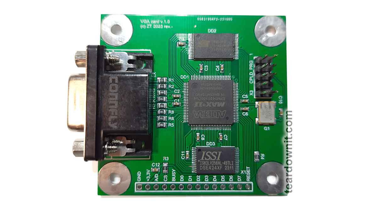
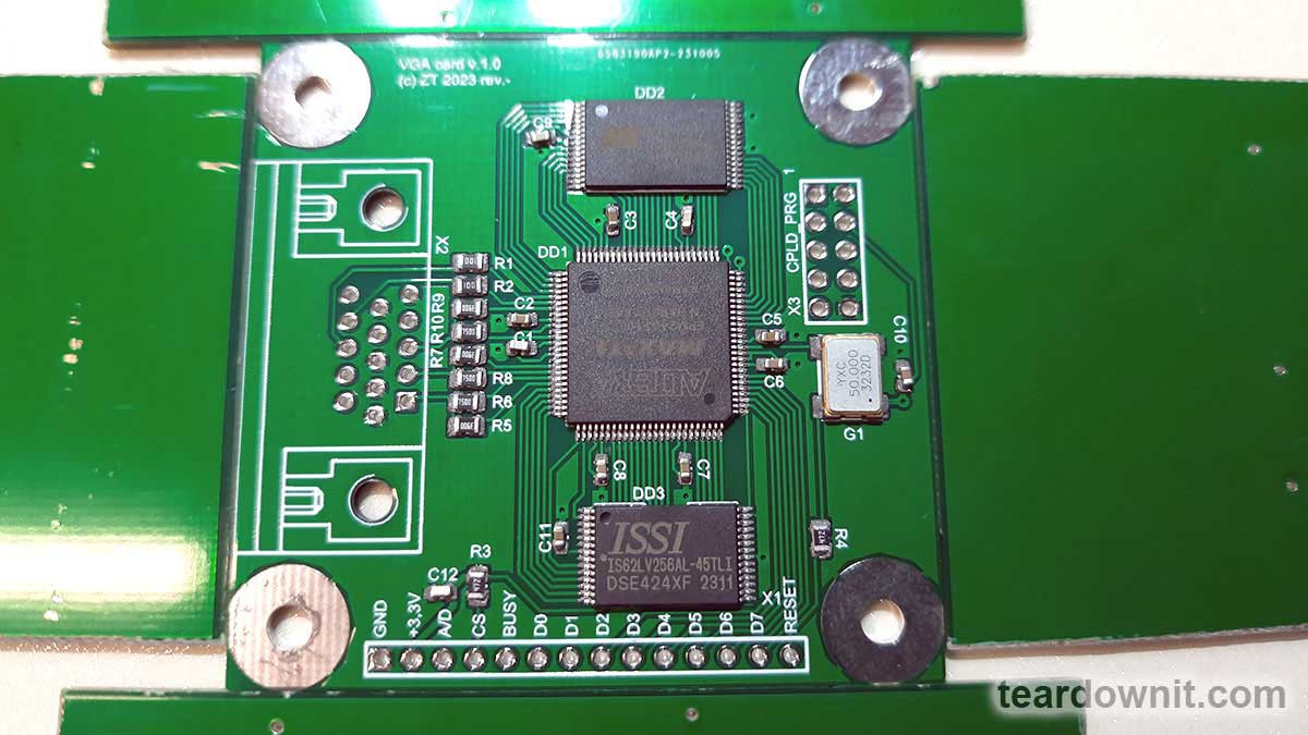
After the final selection of the main components, a printed circuit board, which had specific requirements, was created. The board had to be adapted for manual assembly. Due to this, components were placed on one side of the board, and the number of pinout components was minimized, leaving only external connectors.
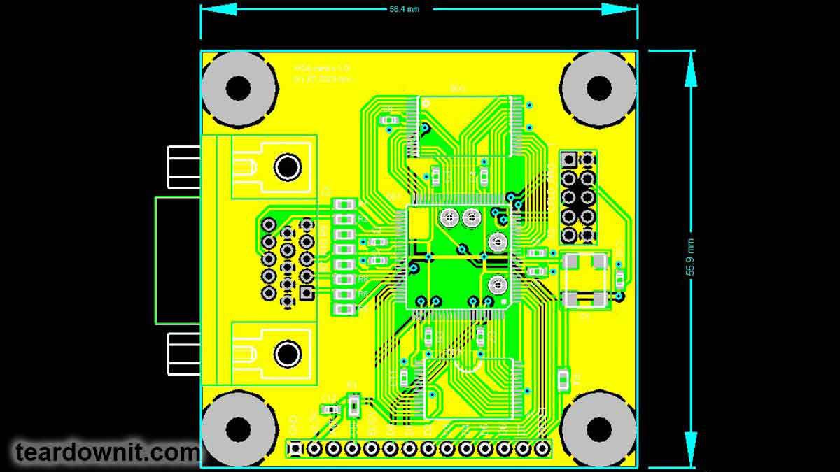
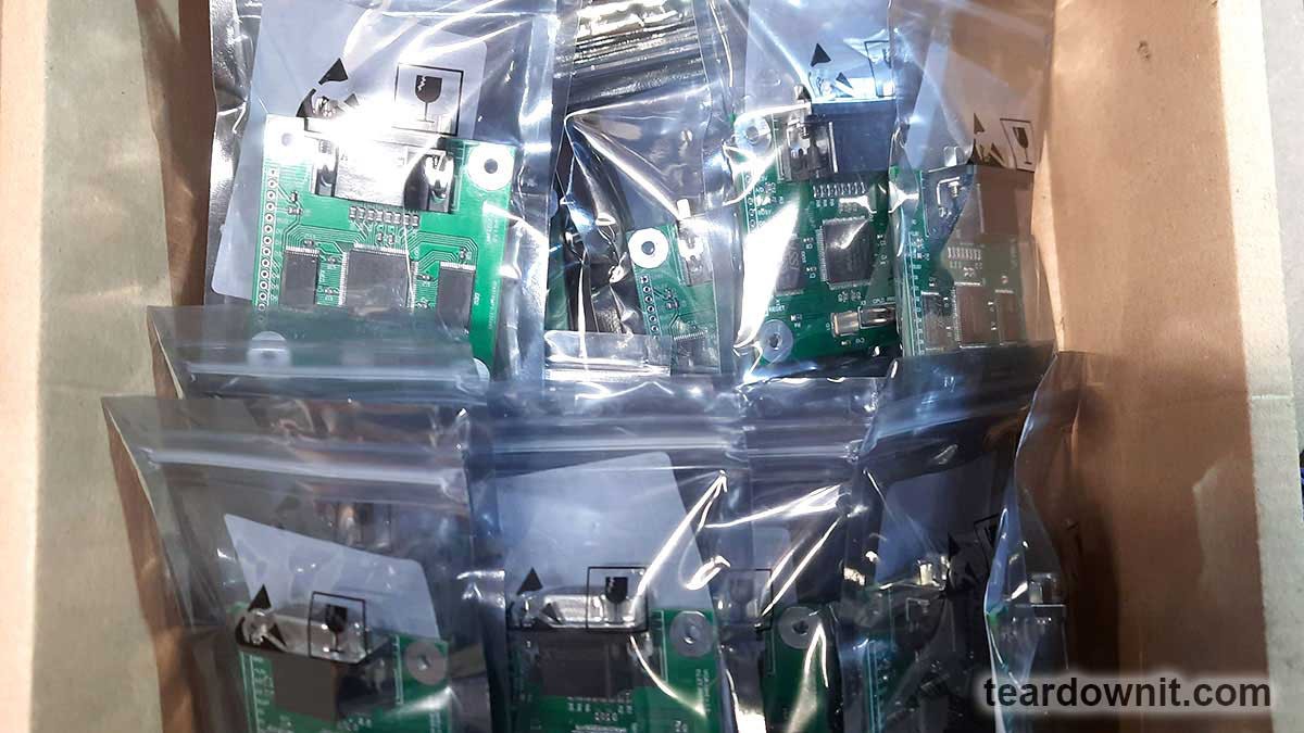
50 copies of printed circuit boards were ordered. This introduces the risk of the first boards' errors and inaccuracies, leading to scrapping all fifty and re-ordering the whole batch. Also, along with the boards, a stencil for applying solder paste was ordered. This will simplify the assembly process.
While waiting for the boards to be manufactured and delivered, it was time to think about flashing and testing the finished boards. Flashing CPLD was less difficult and could be done using a separate connector and USB programmer. However, programming the character ROM seemed more questionable. On a development board, to reprogram the firmware, the chip had to be carefully removed from the breadboard panel, inserted into the programmer, erased, flashed, removed, and returned to the breadboard panel. These operations turned out to be quite labor-intensive.
Therefore, to program the character ROM, it was decided to use the tools of the CPLD itself through a custom parallel interface. There were two possible implementation options:
1. ROM programming with special firmware installed in the CPLD, intended exclusively for ROM programming.
2. Implementation of ROM programming functionality into the working CPLD firmware.
The second option was more complex and required additional CPLD resources that would only be used once or twice in the device's lifetime. Fortunately, there were enough CPLD resources available to implement the second option.
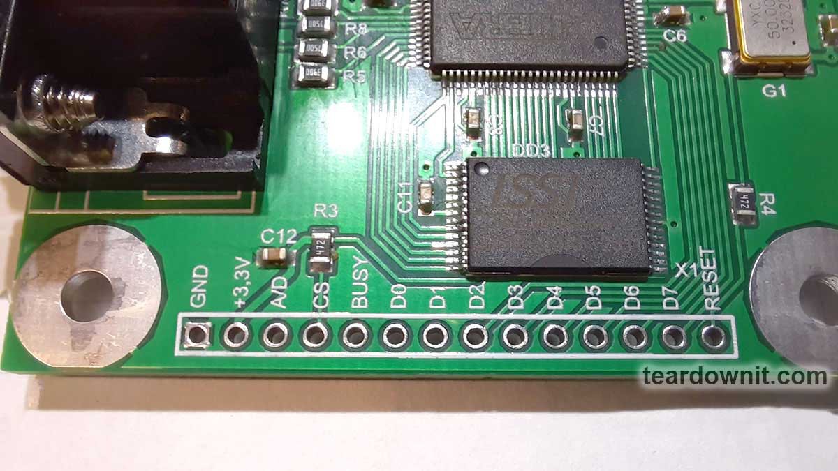
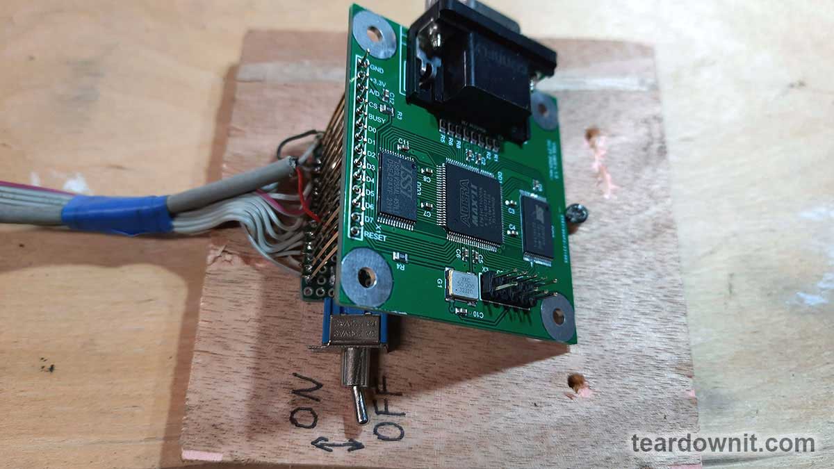
The finished prototype was tested through the same parallel user interface, displaying the test picture on the screen. To do this, I utilized an old laptop with an LPT port, which provided enough I/O lines to transmit all the necessary signals to the device.
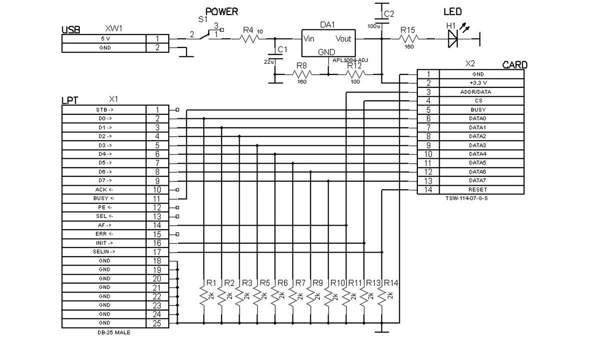
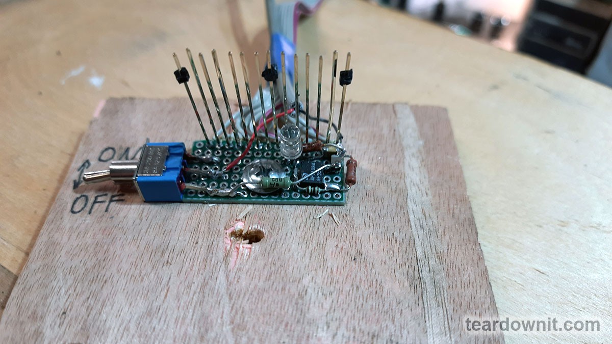
The testing device (diagram above) was assembled on a breadboard using the surface-mounting method. The resistors were installed in the housing of the DSUB25 connector, and the tested or programmed board was connected with long and flexible pins.
When bending, the contacts create tension in the board hole, ensuring reliable contact. 2 kOhm resistors, together with pull-up resistors of the LPT interface (approximately 1 kOhm), form a voltage divider. This divider converts the 5V logic levels of the LPT port to 3.3V ones.
The board is powered through a simple linear stabilizer, getting a voltage of 5 V from the laptop’s USB connector. Resistor R4 with a resistance of 10 ohms is used for current protection. Suppose a short circuit or other problems are on the board under test. In that case, its voltage will decrease, preventing the USB port from overloading. An LED controls a voltage drop of less than 2 V; it will not light up when the power is turned on.
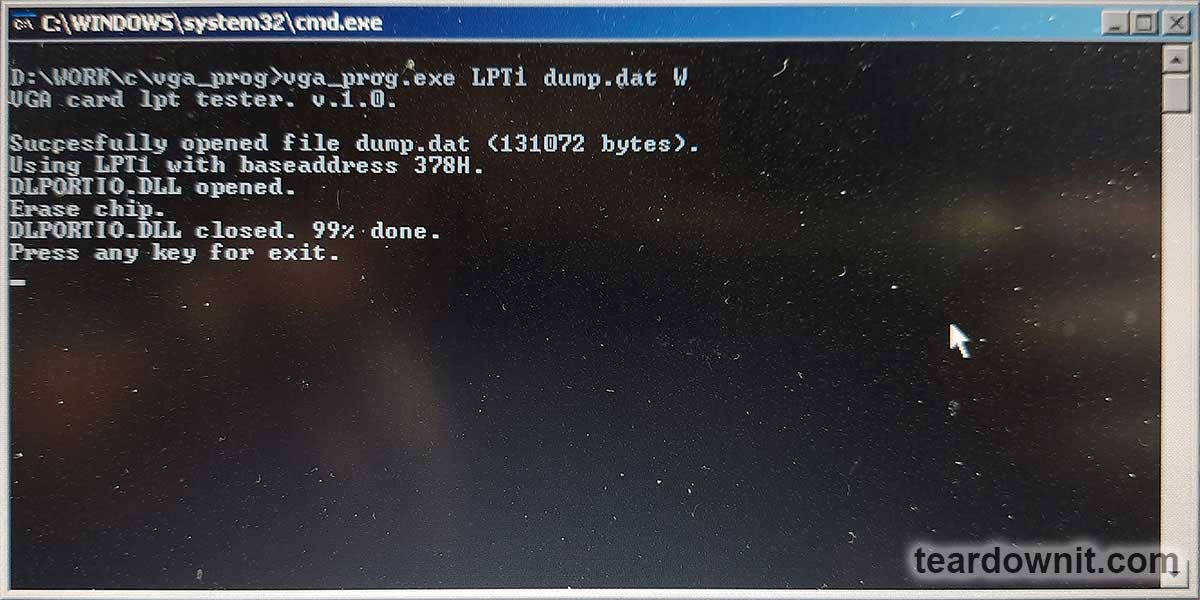
The command-line script for flashing the firmware and testing is written in C. For hardware access to the LPT port, the well-known DLPORTIO drivers are used. It should be noted that these drivers only work fine on Windows XP.
Font files are required to create a dump that will be written to the character generator's ROM. *. FNT files from the MSDOS system or programs of that time are suitable for this. These files contain bit masks of ASCII table characters. For example, in an 8x16 font, each character is described by 16 consecutive bytes.

Modern *. FNT files (as introduced into Windows systems) have a slightly different format. To extract bit masks from them and convert them to the desired format, the script fnt2bin.exe was created. This program takes as input a *. FNT font file with a height of 16 pixels. To convert any other font to the *. FNT format, you can use any free font converter. The result of running the fnt2bin.exe program will be a file of exactly 4096 bytes containing bit masks of the converted font characters. Thus, a dump of the character generator ROM firmware was created, including 32 different fonts.
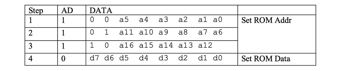
To flash this dump into the ROM using CPLD tools, one of the free bits of the control register was allocated. This bit can only be activated when a RESET signal is present. Upon exiting reset mode, this bit is automatically reset, returning the CPLD to regular operation. After setting this bit, the address setting logic changes, and this address register connects itself to the ROM address bus (not RAM). A 17-bit address is formed in three parts: 6, 6, and 5 bits. The two most significant bits of the address byte determine the "chunk" of the address being written: 00: bits 0 to 5, 01: 6 to 11, 10: bits 12 to 16. Then, one needs to switch to data transfer mode and transfer the data byte written to the ROM chip at the leading edge of the HOST_CS signal. Thus, one packet of address and data to the ROM chip consists of four parts, as shown in the table below.
These messages then form sequences to initiate the byte's flashing. According to the datasheet, there is no "flash completion" flag; it is just waiting for a pause that clearly exceeds the time required for the firmware to flash.
The process is slow, but there is no point in rushing when flashing ROM since writing to the ROM itself takes a lot of time. Additionally, writing to the ROM is typically done only once per device.
During software development, the ordered boards, components, and chips arrived. A homemade device was created for applying solder paste. It has a sturdy laminated wood base with stops from PCB scraps to hold the board in place.
The stops were attached with thin, double-sided tape. A sheet of paper placed under the PCB being processed compensated for the height of the tape. This way, the board became perfectly aligned with the stops.
A stencil is placed atop the stops, and solder paste is applied.
The components are then placed by hand on the applied solder paste.

Positioning the components precisely is unnecessary since they will drift to their respective places due to surface tension during reflow and become nicely aligned. Although solder paste will stick components to the board, care must be taken not to accidentally dislodge already installed components.
Solder reflow is performed using another homemade device.
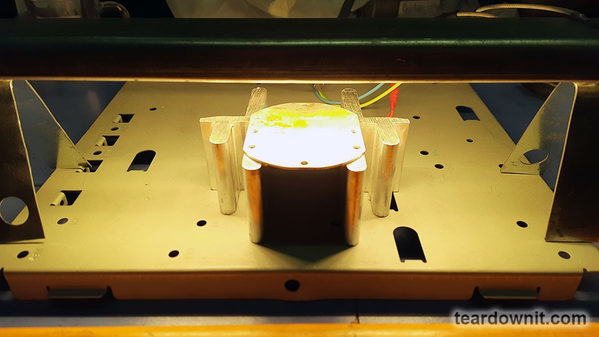
It includes an aluminum heater based on a 300 W thermistor from AliExpress and an IR lamp from the grill of a faulty 600 W microwave oven. Melting occurs very quickly, literally within a few seconds.
During reflow, it is essential to keep a close eye on the components and, if necessary, use tweezers to help them move into place, especially if they are not attracted to their pads. If a solder bridge forms on two pins of a chip with a fine pitch, it must be removed using copper braiding.
After soldering the surface-mount elements, installing the output elements, such as two connectors, is time. After soldering, a visual inspection is performed, and the remaining flux should be washed off.
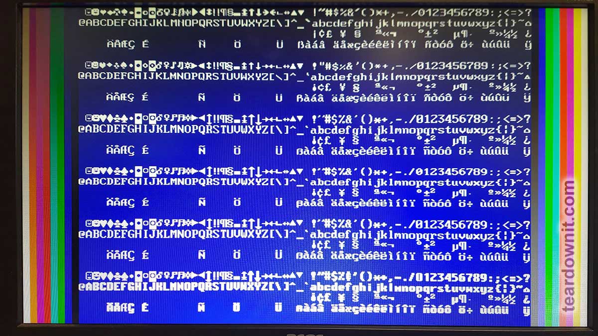
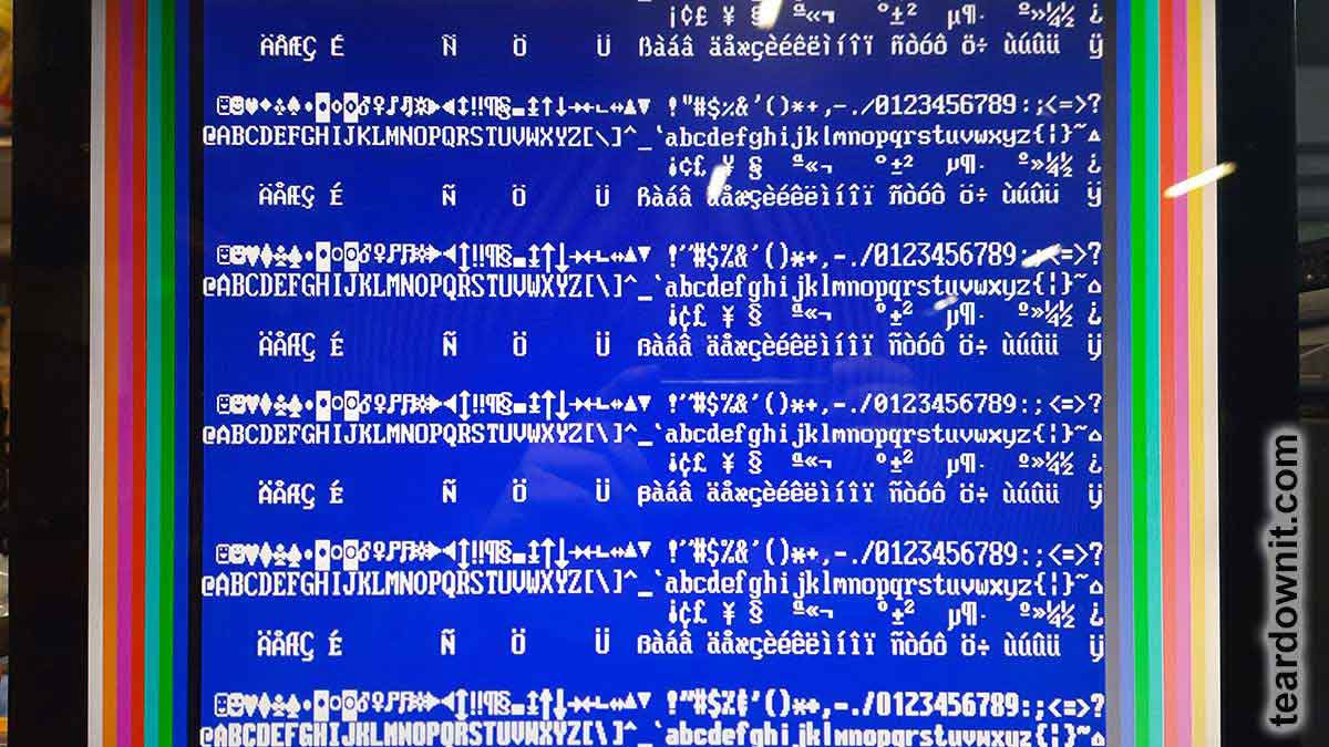
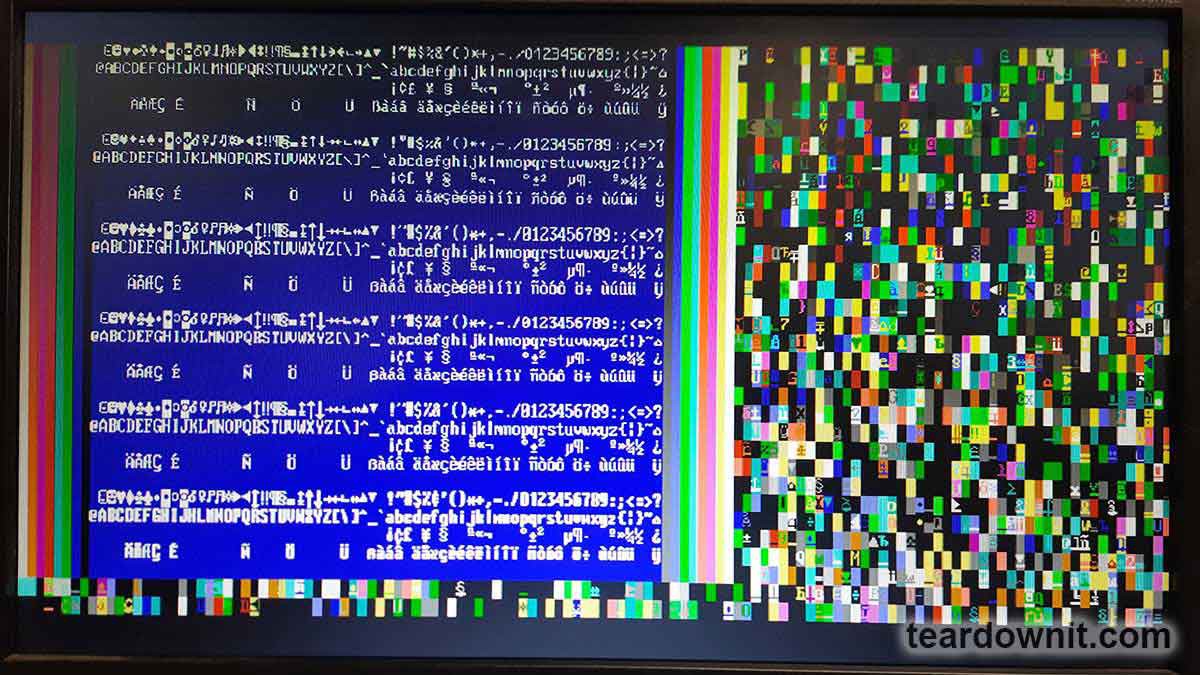
After these steps, the board is installed into the fixture for programming and testing. The test picture is shown in the photo below.
After removing the pin shorts and cleaning, it became evident that only 7 out of 20 boards worked. The rest required a more careful inspection for shorts and problematic soldering connections. As a result, 19 boards started working successfully. Still, one board had to be disassembled and reassembled on a new circuit board, and only then was it operational.
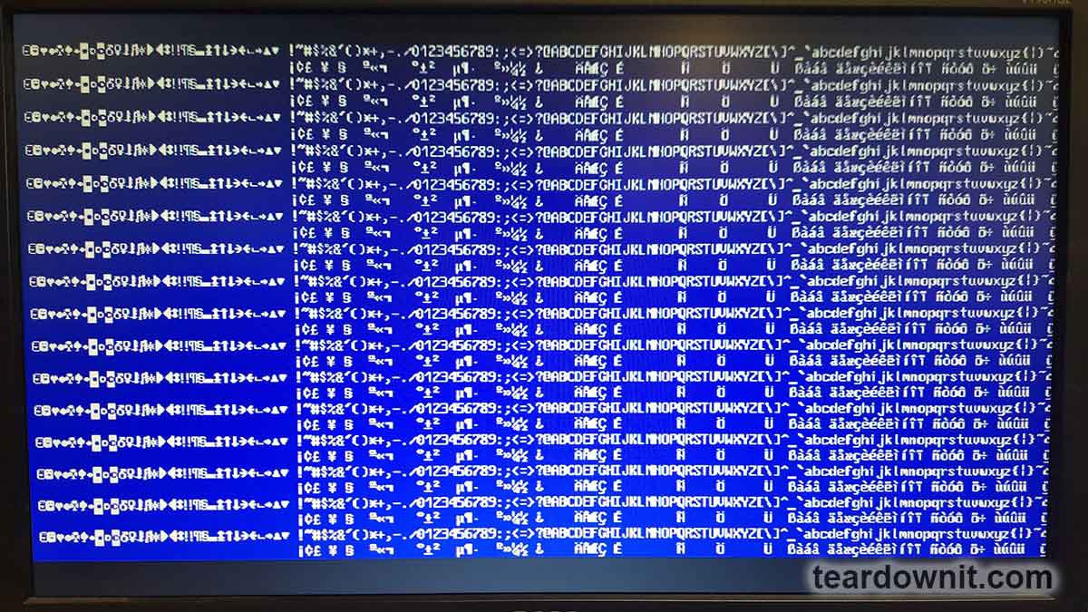
While working on the board, another idea arose: to use all the device's RAM for 128 characters in 32 lines. This mode would look better on widescreen monitors. This is what the test picture looks like on a widescreen monitor—too much horizontal stretch.
A temporary firmware was written for CPLD for testing, implementing a non-standard 1024×576 mode. This mode is not on the list of standard supported resolutions.
The horizontal parameters were taken from the 1024×768 43 Hz mode and the vertical parameters from the 768×576 60 Hz mode. At a pixel frequency of 50 MHz, the horizontal frequency was 39.55696 kHz, and the refresh rate was 66.25957 Hz. Both of these values are within the acceptable range; for example, the Acer V196HQL monitor, and this monitor displayed the image.
The photo below compares an area of 80×30 characters and an area of 128×32. The number of characters is 1.7 times greater.
However, in this mode, 32 lines of characters use just 512 vertical pixels out of 576. Consequently, 2 lines at the top and 2 lines at the bottom of the image remain empty, and the characters themselves become small and less clear due to the discrepancy between the output and the monitor's native resolution.
Since this mode is non-standard, you cannot be sure it will work on all monitors. However, with a high probability, it can be assumed that there will be no issues if the operating frequencies fall within the permissible range.
The timing diagram for this version is:
Discussions
Become a Hackaday.io Member
Create an account to leave a comment. Already have an account? Log In.