Andy
AndyDisclaimer:
This device is not an accurate measuring device and is intended to estimate the current consumption of the load in dynamics. The measurement error may vary within 1-2 discrete units.
And please excuse my English (I am from Ukraine and my native languages are Russian and Ukrainian).
Development history and a little bit of theory
Sometimes I have to develop and test various autonomous devices. And one of the main requirements for an autonomous device is low power consumption.
Accordingly, there is a need to measure the current consumed by the device. If it is a device that consumes power constantly - you can take a multimeter and simply measure the current consumption.
What if the device is in power saving mode most of the time and only occasionally switches to active mode for a short time? Then the multimeter will not help, because it will not be able to measure the short-term increase in consumption normally.
As an option, you can include a shunt in the power supply circuit of the device and connect it to the ADC through an appropriate amplifier. The converter will sample the current consumption. Samples can be taken quite often, for example, every millisecond. And then these samples can be saved for further analysis.
And if the shunt is built into the feedback circuit of the voltage stabilizer, the voltage drop across the shunt will not affect the supply voltage of the device under test.
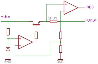
This is an example of a simple voltage stabilizer. The output voltage is compared to the reference voltage through a divider, and an operational amplifier generates the control signal for the regulating transistor. The voltage drop across the shunt does not affect the output voltage because the shunt is included in the feedback circuit.
The voltage across the shunt is amplified and fed to the ADC.
Everything looks very nice, but the first questions arise when selecting the shunt resistance. After all, the device under test can consume 1-2-5 µA in standby mode and up to 50-100-200 mA in active mode.
If you take a shunt with a small resistance, the voltage drop across it at low currents will be small. This voltage will be difficult to amplify without being affected by noise and interference. If you take a shunt with a large resistance, the voltage drop across the shunt will be quite high at high currents. Which will require a fairly high input voltage. In addition, the shunt will heat up due to the high power on it. And heating of the shunt can cause a change in its resistance, which will negatively affect the accuracy of measurements.
Consider a shunt with a resistance of 1 ohm. At a current of 100 mA, the voltage drop across the shunt will be 100 mV and the power will be 10 mW. This voltage is sufficient for amplification and further sampling.
Now let's see what happens at a current of 1 µA. The voltage drop will be only 1 µV. This is quite a small voltage and a low noise amplifier is needed to amplify it. Interference protection measures must also be taken.
We can try to take a 100 ohm shunt. Then at a current of 1 µA the drop will be already 100 µV. This voltage is much easier to amplify and filter out interference.
But at a current of 100 mA on the shunt will be a voltage drop of 10 volts. And the power will be 1 watt. That's a lot.
There is another aspect to consider - the resolution of the ADC. The range of 1 µA - 100 mA with a step of 1 µA is 100000 points. That is, you need an ADC with a resolution of at least 17 bits (131 thousand points). And to reduce the influence of noise and errors it is desirable to take 18...20 bit ADC and for each point make several samples and then average them. Such ADCs with speed not less than 2000-4000 SPS are rather expensive. With such ADC it is necessary to use a low impedance shunt, low noise amplifier and take measures to reduce noise.
You can try this variant. You need to take two shunts and switch them depending on the current consumption. And switch them automatically.

It remains to decide how to switch the shunts.
The above circuit is quite difficult to implement. It is necessary to have some fast-acting switch, so that it can react even to short pulses of current consumption. And every time you need to remember which shunt data is fed to the ADC.
Let's try to change that circuit.

Here we have connected two shunts in series. The first, low impedance shunt is for measuring large currents. The second shunt with higher resistance is for measuring small currents.
And the signal from the amplifier of the first shunt controls a key that allows the current to bypass the second shunt. You can try to use a field-effect transistor as such a key.
It is necessary to invent some threshold circuit controlling this transistor.
You can try to use a silicon diode as an automatic key. Its threshold characteristic in the low voltage region is ideal for us.
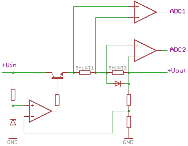
The diode is placed in parallel with the second shunt. As the current increases, the voltage drop across the shunt will increase. And starting from a certain point, the diode will open and allow part of the current to pass through itself. That is, at all currents, the drop across the second shunt will be limited by the drop across the diode. For a silicon diode this voltage is about 600-700 mV.
The disadvantage of splitting the measurement into two ranges is a coarser measurement at the high-current shunt.
Let's take the first shunt with a resistance of 1 ohm. This shunt will measure currents in the range of 1 mA and above. The second shunt, with a resistance of 200 ohms, will be used to measure small currents, up to 1 mA. At a current of 1 mA, there will be a voltage drop of 200 µV across the shunt. And at a current of 1 mA, the voltage drop will be 200 mV. At this voltage, the silicon diode is closed and has no effect on the shunt current. The diode will begin to open at a voltage of about 350-400 millivolts. It will fully open when the voltage reaches 600-700 mV, limiting the voltage across the second shunt.
Current measurement on two ranges will allow the use of cheaper ADCs.
Low-current range 0 - 1000 µA in 1 µA steps, high-current range 0 - 200 mA in 0.1 mA steps.
Even a 12-bit ADC built into the STM32 will be sufficient for these ranges.
There is also one nuance here. The feedback divider of the stabilizer is connected after the shunts. Current flows through it, which also creates a voltage drop across the shunts. This can be a problem. But in digital data processing, this drop can be calculated and compensated for. Since this drop depends linearly on the output voltage of the stabilizer, it is necessary to measure the output voltage synchronously with the сurrent measurement.
After this theoretical research and simulation in Proteus software, I moved on to the modeling phase.
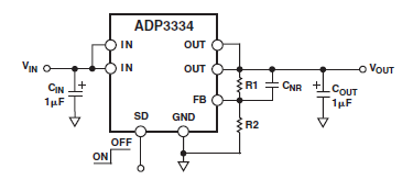
As a stabilizer, I took an ADP3334 from Analog Devices with a separate feedback input, which allowed me to make an adjustable stabilizer and include shunts before the feedback divider.
I used a high input impedance AD8626 precision dual channel operational amplifier (also Analog Devices) as the signal amplifier from both shunts.
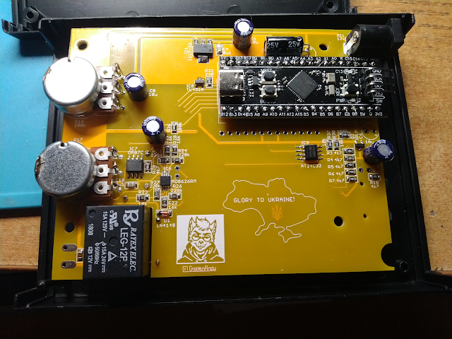
Data sampling and processing was performed by the STM32F411CE microcontroller on the debug board (BlackPill).
I was satisfied with the test results and it was time to create a finished device.
The microcontroller does not control the stabilizer in any way, but only acts as a meter and recorder. I.e. in essence it is an analog regulated power supply to which a digital voltmeter and a digital milliammeter are connected.
Experiments have shown that the measurement results are affected by interference from my cell phone. Therefore, in the finished device, it may make sense to cover the area of the stabilizer and operational amplifiers with a tin shield. The shield should be connected to a common wire (minus power supply). For example, to pin 39 of the microcontroller board......
Schematic.
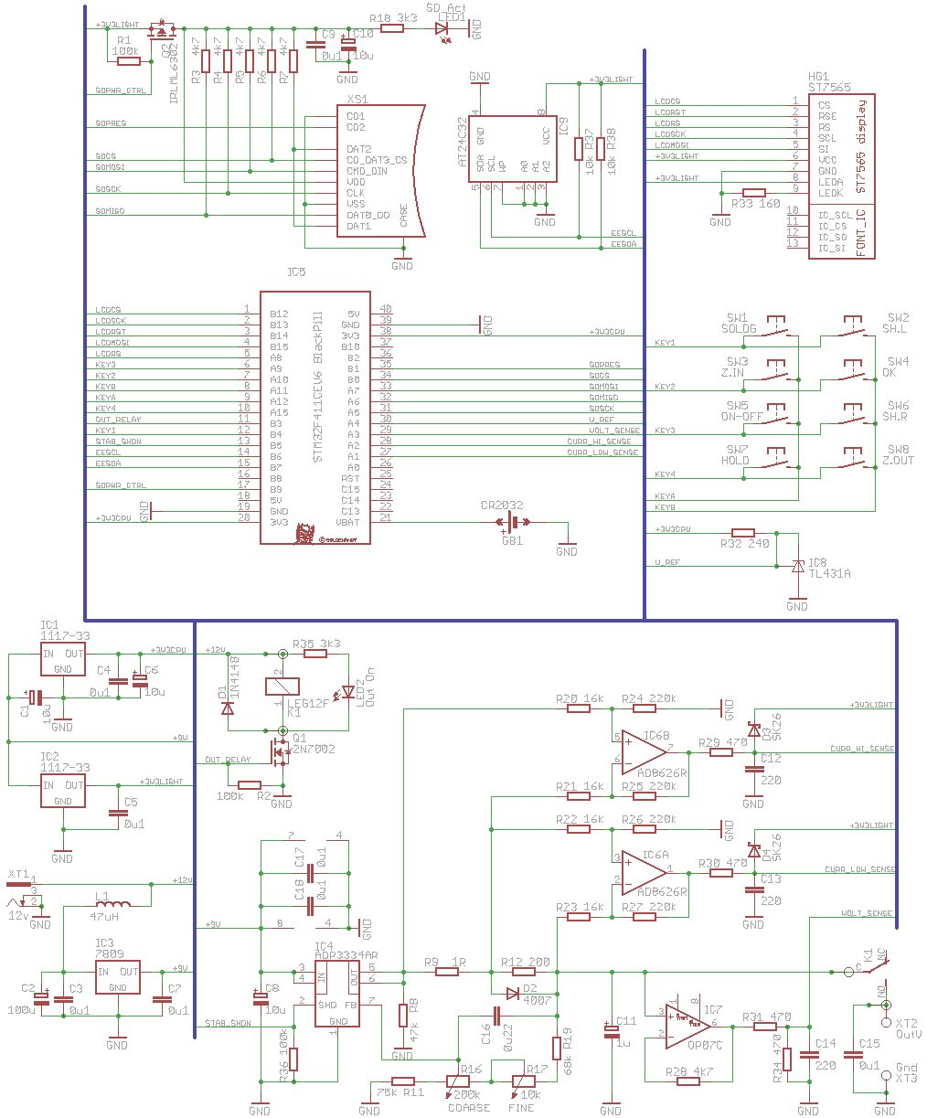
Circuit power supply.
The device is powered by 12 volts. These 12 volts are fed to the input of the device and through a filtering choke are fed to the linear stabilizer IC3. The output of this regulator is 9 volts, from which the entire analog part of the device is powered by. The unfiltered 12 volts are used to power the relay that turns the output on and off.
Analog part.
Stabilizer IC4 - ADP3334, included according to the typical circuit. The feedback divider includes 4 resistors. 2 variable resistors with linear characteristic (B) are responsible for coarse and fine adjustment of the output voltage. The resistors are selected so that the output voltage is regulated in the range of 1.5 - 5.5 volts. C16 is a filter, R8 is a load resistor for normal operation of the stabilizer.
The ADP3334 has an operating current of 500 mA and a peak current of up to 800 mA. The output current is software limited at 250 mA. If this current is exceeded, the power supply output will shut down within one second.
Note that the continuous output current of the device is determined by the power dissipation of the ADP3334, at an output voltage of 1.5 volts the recommended average current should not exceed 65 mA, at 5 volts it should not exceed 125 mA. These are calculations for a power dissipation of 500 mW. The ADP3334 has built-in over-temperature protection; at 165°C, the stabilizer shuts down. For better cooling, there is a small unmasked copper polygon under the stabilizer. When mounting the ADP3334, you can also try applying a small amount of thermal paste to the bottom surface of the IC. There is no separate short-circuit protection.
Shunts. Resistor R9 is a high-current shunt. Resistor R12 is a low-current shunt.
Operational amplifiers IC6A, IC6B are amplifiers of the signal from shunts. Differential amplification circuits are used. For correct operation of amplifiers it is necessary to select as accurately as possible pairs of resistors: R20 and R21, R22 and R23, R24 and R25, R26 and R27. The absolute value of the resistors is not as important as the identity of the pairs.
The resistors are selected so that the shunt voltages in the operating current ranges fall within the microcontroller ADC range.
From the amplifiers output through filters R29C12 and R30C13 the amplified signal goes to the microcontroller ADC.
Operational amplifier IC7 is a high impedance repeater for voltage measurement. R31R34C14 - filtering and bringing the output voltage to the microcontroller ADC range.
Relay K1 turns the output of the device on and off.
Digital part power supply.
The microcontroller and display are powered by stabilizer IC1.
Stabilizer IC2 provides separate power for the display backlight and SD card.
When the voltage on the shunts increases, the output voltage on the IC6 amplifiers may exceed the microcontroller ADC range of 3.3 volts. In this case, the excess voltage will flow through diodes D3D4 into the power supply bus of the display backlight and SD card, raising them to about 3.5 volts. That is why two separate power regulators are used, one for the microcontroller and one for the card and display backlight.
Digital part.
The microcontroller provides measurement and recording of current and voltage values. STM32F411CE microcontroller on the debugging board (BlackPill) is used. Signals from shunt amplifiers and voltage repeater are connected to analog inputs of the microcontroller.
The microcontroller in the applied package uses the supply voltage as the reference voltage.
Since the stability of IC1 voltage may be insufficient, a separate reference voltage source IC8 - TL431A is additionally connected to the microcontroller. Its stability is much higher than that of stabilizer IC1. This allows the possible voltage instability of IC1 to be corrected by software.
Every millisecond, the microcontroller performs several series of voltage captures on the analog inputs. These values are then averaged and, if necessary, corrected. Next, the output voltage of the stabilizer and the current consumed by the load are calculated.
The obtained current consumption values are stored in the microcontroller's RAM buffer.
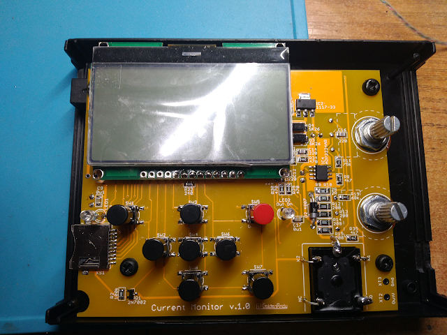
The information is displayed on a monochrome LCD display with a resolution of 128x64 pixels and Sitronix ST7565 controller.
A microSD (TF) memory card slot is also connected to the MC. This allows the captured current and voltage values to be saved to the memory card. The data is saved at a sampling rate of 1000, 500 or 250 times per second. The saved data occupies 1 - 1.5 mb/minute at 1000 samples per second. You can also enable averaging every 10 or 50 values and saving the averages to a memory card. This will reduce the file size saved to the memory card.
The IC9's EEPROM memory is used to store settings and calibration data.
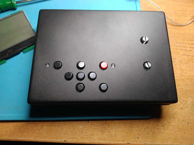
The device is controlled by buttons SW1-SW8.
Parts and their replacement.
MCU. There are no options here - BlackPill with STM32F411CE chip. For example, here.

Display. 128*64 resolution, ST7565 controller, 2.2" diagonal, SPI interface. For example, here.

Display must be on a transition board, three-volt version (without stabilizer).
SD/TF memory card slot. A simple slot without a latch with extra pins to detect the presence of a card. For example, here.

Stabilizers. AMC1117-33 in SOT-223 package, 7809 in SOT89 package.
Choke. The choke filters noise from the external PSU. Choke case - 4D18 (CDRH4D18), inductance - the bigger the better. The minimum current of the choke is 500 mA.
Relay. LEG-12 or similar. One switching or normally open contact pair, 12 volt DC coil. For example, here or here.
IC6 - shunt signal amplifier. AD8626 is a precision low-noise rail2rail dual-channel operational amplifier with CMOS inputs. It can be replaced with something similar and pin-compatible. Requirements - single gain at 2 MHz and above, CMOS inputs, r2r, power supply of at least 10 volts (+/-5V), low noise.
Note that the AD8262 is available in an MSOP package. This package is pin-compatible with SOIC, but requires PCB correction for this package.
IC7 is a supply voltage repeater. OP07C from Texas Instruments. Here the requirements for the op-amp are lower. Single gain of 1 MHz, low drift and offset.
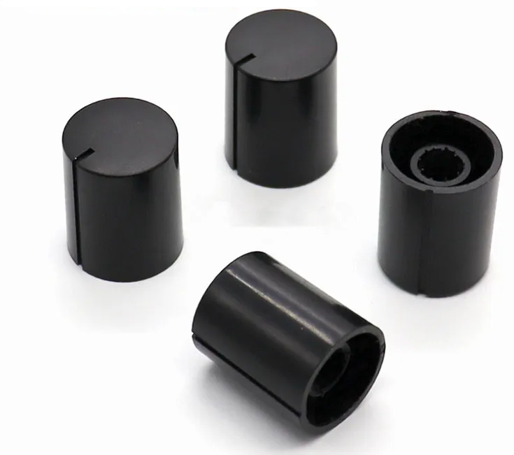
Adjustment resistors. 200 kOhm and 10 kOhm resistors with linear characteristic (B). I used these:

I used these knobs for the resistors:
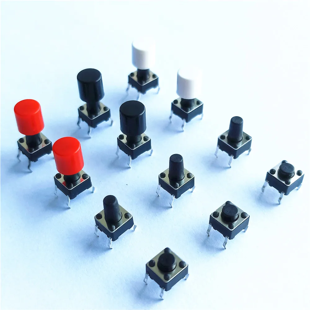
Buttons. The tactile buttons are 6x6mm for surface mounting. I used 12mm height buttons. For example, here.
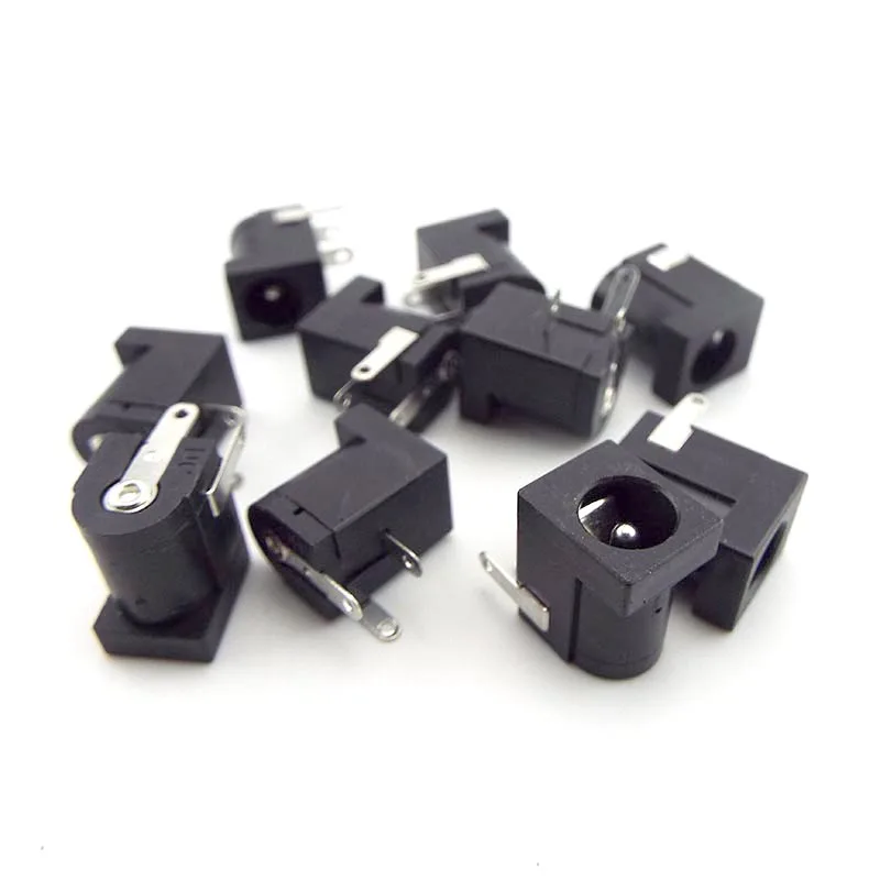
Input power connector. 5.5x2.1 mm DC power connector for PCB.
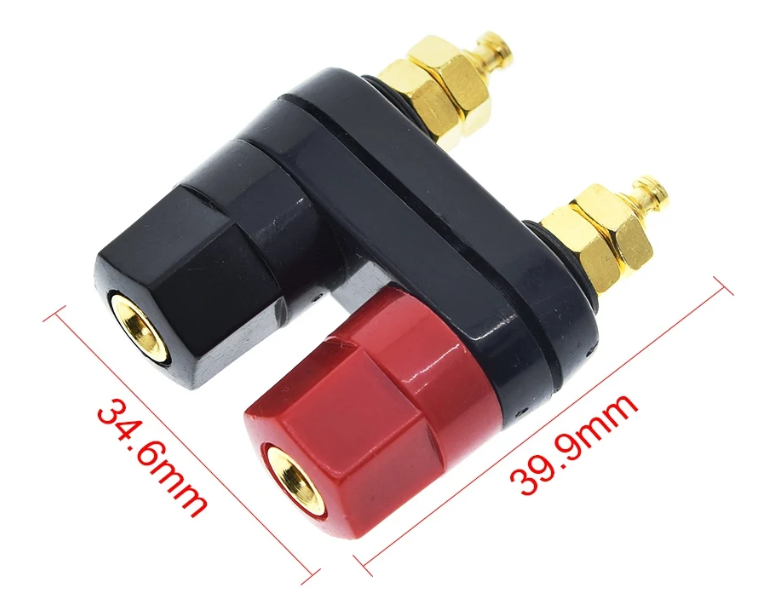
Output terminals. I used these 4mm "bananas".
PCB
The board is presented in two versions - for homemade and for factory production. In the homemade version the transition vias diameter is increased. Additional transition vias are added for parts that are difficult to solder from the mounting side (capacitors, microcontroller board, display, etc.).
PCB images (factory production version).


The boards are designed for the Z-19 case made by Maszczyk, Poland.
Similar enclosures are available from other manufacturers, e.g. Kradex.
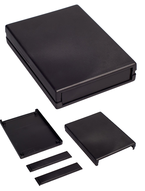
The dimensions of the case are 129x94 mm and the height is 25 mm.
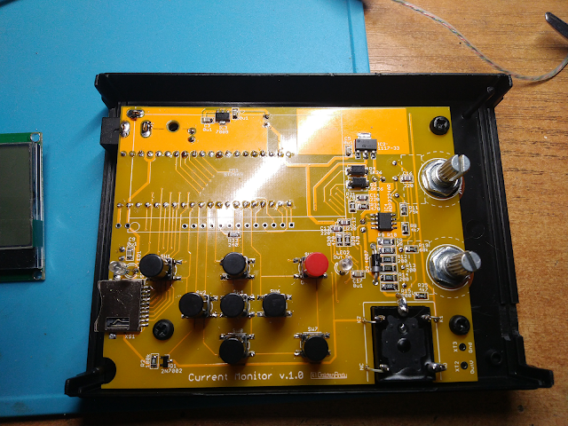
Checking the arrangement of the device parts
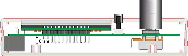
The printed circuit board is mounted in the provided locations using 6 mm nylon standoffs. This mounting allows the power connector to be placed on the underside of the board. The voltage regulation resistors are mounted directly on the board. They are connected to the board with a mounting wire.
The only problem with this enclosure is that the Rayex LEG-12 relay used does not fit over or under the board. A smaller relay could be used. But I already had LEG-12 relays. So I provided a cutout in the board to allow the relay to be mounted on the mounting wires.
Both mounting options for this relay are provided on the board.

Gerber files for factory production.
Gerber files for homemade board.
Firmware.
The firmware is loaded into the microcontroller using ST-Link v2 programmer and STM32 ST-LINK utility.
To load the microcontroller firmware it is necessary to connect 3 lines to the programmer - Gnd, SWDIO and SWCLK. It is also necessary to supply power to the MCU.
1. Connect the device to the programmer
2. Connect the programmer to the computer
3. Start the ST-LINK Utility program.
4. Select the menu item Target - Connect
5. After successful connection, select the Target - Erase chip item
6. File - Open file - select hex file with firmware.
7.Target - Program & Verify
8. After successful flashing: Target - Disconnect
Firmware, version 1.0.526.
User manual.
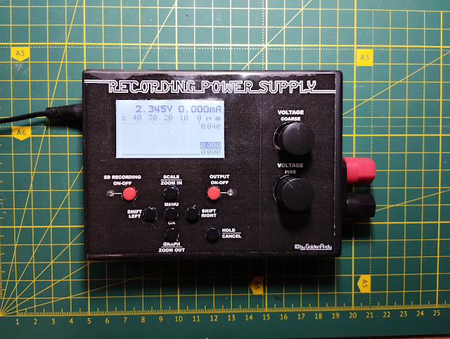
When you turn on the device, the main mode screen appears after the splash screen.
The screen is divided into several areas.
Operational values area (highlighted in red). The output voltage of the device and the load current are displayed here. If a memory card is inserted in the slot, the corresponding symbol is displayed on the left.
The remaining areas refer to the stored load current values.
The blue area is a graph of current consumption over 50, 100 or 200 seconds. At 1000 counts per second it is 50 seconds, at 500 SPS it is 100 seconds, and at 250 SPS it is 200 seconds.
The graph area is divided by dots into squares. Each square is equal to 5, 10, or 20 seconds. The green area is the graph time scale in seconds. The current time is also displayed here.
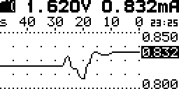
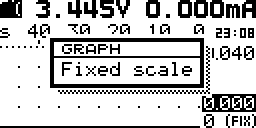
Yellow area - graph range in milliamperes. The upper limit is selected automatically by the maximum current stored in the buffer.
The lower limit depends on the scaling mode. It is either always zero (fixed mode) or is selected by the minimum current value stored in the buffer (adaptive mode). In fixed mode, the lower limit of the graph is signed as 0 (fix).
The current corresponding to the right side of the graph is also displayed in this area. This current is displayed in inverse mode.
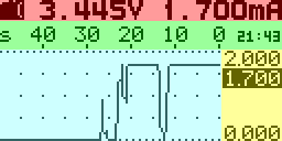
An example of an adaptive lower limit. It can be seen that the current varies from 810 to 832 µA. The limits have been automatically selected to show the most detailed graph.
Pressing the On/Off button turns the load on and off. The LED indicates that the load is on.
Current consumption values are permanently stored in the built-in 50,000 value buffer, replacing the oldest values.
Pressing the Zoom In button toggles the vertical graph scaling mode - fixed or adaptive. The corresponding information message appears.
Pressing the Zoom Out button toggles the graph mode - averaging or minimum+maximum. This is necessary when there is more than one buffer value per graph point (in the main mode there are 500 buffer values per graph point). In the averaging mode, the buffer values are averaged and then a single graph point is plotted. In the minimum+maximum mode, a vertical line is drawn on the graph from the minimum to the maximum value.
When the graph mode is switched, the corresponding information message is also displayed on the screen.
Scaling and graph modes can also be toggled via the settings menu.
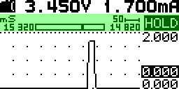
When the Hold button is pressed, the device enters the data buffer view mode. The saving of new data in the buffer is suspended.
In the buffer view mode, the visible range of buffer in milliseconds is displayed in the timeline area.
The scroll bar is also displayed there, when zoomed in. Just above it, the number of milliseconds for the graph cell is displayed.
Flashing HOLD indicates the buffer view mode.
In this mode, toggle scaling and display modes is possible only through the settings menu.
When zooming in, the graph limits are adjusted to display the graph's visible part in as much detail as possible.
In the buffer view mode, the Zoom In/Zoom Out buttons change the graph scale. The maximum zoom is 10 buffer values per graph cell (one buffer value per display pixel).
The Shift left/Shift right buttons move the graph left and right.
Pressing the On/Off button turns the load on and off, but does not disable the buffer view mode.
Pressing the Hold button again returns the device to the main mode and resumes buffer recording.
In both of the above modes, the Ok button opens the settings menu.
Use the Zoom In/Zoom Out buttons to select a menu item.
The Ok button changes the selected menu item.
Hold button - exit the menu or cancel in the editor windows.
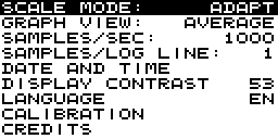
The first two menu items toggle the scaling and display modes.
The third menu item, SAMPLES/SEC, is a count of current samples per second. Pressing the Ok button cycles through the values 1000, 500 and 250.
The next menu item, SAMPLES/LOG LINE, is averaging data when recording to a memory card. Pressing the Ok button cycles through values 1, 10, and 50. This item is not available when data recording is in progress.
The DATE AND TIME menu item is used to set the time. Pressing the Ok button opens the date and time editor:
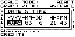
Shift left/Shift right buttons select the value to be changed, Zoom In/Zoom Out buttons change it.
Ok button saves the date and time, exit without saving - Hold button.
The DISPLAY CONTRAST menu item is used to adjust the display contrast. The Zoom In/Zoom Out buttons adjust the display contrast. The Ok button saves the new contrast value, and the Hold button exits without saving.
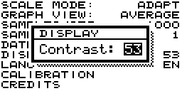
You can also enter the display contrast adjustment mode by holding down the Shift left button while turning on the device.
CREDITS menu item - firmware and author information.
Calibration of the current and voltage meter.
The CALIBRATE menu item allows you to calibrate the current and voltage meter. This item is not available when data recording is in progress.
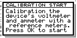
Calibration requires the most accurate voltmeter, a milliammeter, and resistors of about 100 ohms and 2 kOhm.
Calibration is performed in four steps.
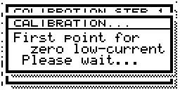
1. The voltmeter is calibrated at two points, 1500 and 5000 millivolts. Calibrate at the first point: Connect the voltmeter to the device and set the voltage to 1500 millivolts, then press Ok.
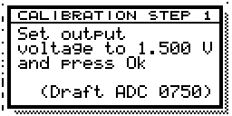
The display will show the draft ADC value of the voltmeter, the normal range is 700-800 ADC units.
After pressing the Ok button for a few seconds, the first point for the voltmeter and the first zero calibration point for the current meters will be saved.
The corresponding messages will appear on the display.
2. The second calibration point of the voltage meter.

Everything is exactly the same as the first point, but you must set the output voltage to 5000 millivolts and press Ok. This will save the second point for the voltage meter and the second zero calibration point for the current meters. The normal ADC draft value is 2450-2550 units.
3. Calibration of a low-current meter.
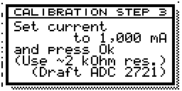
Connect a resistor of about 2 kOhm to the device through an accurate milliammeter and set the current to 1000 µA (1 mA). The normal draft value of the ADC is 2700-2800 units. After pressing the Ok button for a few seconds, the data for the low current meter will be saved.
4. Calibration of a high-current meter.
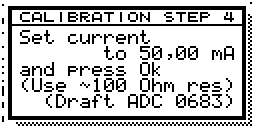
Connect a resistor of about 100 Ohm to the device through an accurate milliammeter and set the current to 50.00 mA.
The normal draft value of the ADC is 620-730 units.
After pressing the Ok button for a few seconds, the data for the high current meter will be saved.
After completing step four, a summary of the measured ADC values will appear.

Recording to SD(TF) card. are calibration values for the zero points of the current meters, they are calculated in the first and second steps. They are used to compensate the parasitic current through the voltage regulator feedback resistors.The Ok button saves the measured values in the EEPROM.
At any time by pressing the Hold button, it is possible to exit the calibration mode without saving changes.
Recording to SD(TF) card.
Recording to the card is turned on and off with the SD LOG button. Recording works independently of the device mode and does not stop when switching to buffer view mode.
The LED indicator shows that recording is on. It is not recommended to remove the memory card from the device during recording! Doing so may damage the file system and cause data loss.
The data is saved to text files named LOGxxxxxx.TXT, where xxxxx is a numeric counter from 00001 to 99999. Before starting to write, the device searches the memory card for the file with the maximum number, adds one to it, and starts saving to the file with the new number.
In the file, the first three lines contain information about the file and the date it was created.
The fourth line is an indication of the units.
All subsequent lines are the millisecond counter, voltage, and current, separated by a tab character.
File example:
#    Supply Current Monitor 1.0.524 log file
#    (c) 2024 by GoldenAndy
#    Log started at 2024-03-06 23:34:48
ms    mV    uA
1    1600    820
2    1600    821
3    1600    820
4    1600    820
5    1600    820
6    1600    821
7    1600    820
8    1600    821
9    1600    820
10    1600    820
11    1600    821
12    1600    821
13    1600    820
14    1600    821
15    1600    821
16    1600    821
17    1600    820
18    1600    821
19    1600    821
20    1600    820
These files can be loaded into a spreadsheet editor (MS Excel and others) for further analysis and processing.

On the graph you can see the noise error of the ADC 😕
Screenshots.
To avoid taking photos of the device screen and drawing pictures in the editor, I added to the device the ability to save the screen image to a memory card.
All screen images above are actual images saved by the device itself.
Since this feature can be useful, I left it enabled permanently.
The screenshot is saved to the memory card when the KEY button on the microcontroller board is pressed.
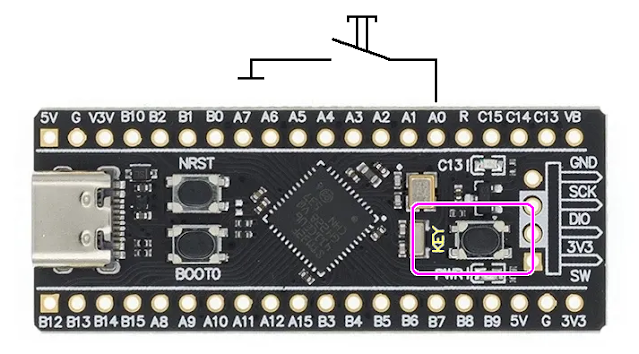
To easily use this feature, you can take a separate button and connect it to pin A0 of the microcontroller board.
Screenshot files are saved on the memory card. Screenshot names are SCRxxxxx.BMP. xxxxx - numeric counter from 00001 to 99999. Searching for a number for a new snapshot is similar to searching number for data files.
Photos.