 Bud Bennett
There has been a lot of DIY effort to make a good, cheap constant current electronic load. I must give homage to the efforts of past attempts, mostly successful, to create something useful for evaluating a power supply's capability or a battery's capacity. It's not easy.
One of the best is Dominik's: https://github.com/Dominik-Workshop/Electronic_load/tree/master
His implementation covers most of the bases and we used it as a benchmark. But it is a bit lacking in user stupidity protection. (And we wanted more.)
Another implementer worth mentioning (besides our eminent Hackaday colleagues) is John Sculley with his excellent treatise on YouTube: https://www.youtube.com/playlist?list=PLUMG8JNssPPzbr4LydbTcBrhoPlemu5Dt
But alas, Mr. Sculley descends into the mire of fixing unforeseen predicaments in a seemingly never-ending fix-it scenario. I guess a nice way of putting it is "Feature Creep".
We recommend viewing Kerry Wong's excellent YouTube videos (https://www.youtube.com/watch?v=WUPrj03UbTM) on Linear MOSFETs for an education in the reality of "Safe Area of Operation", or SOA, for the uninitiated.
A Bit of History
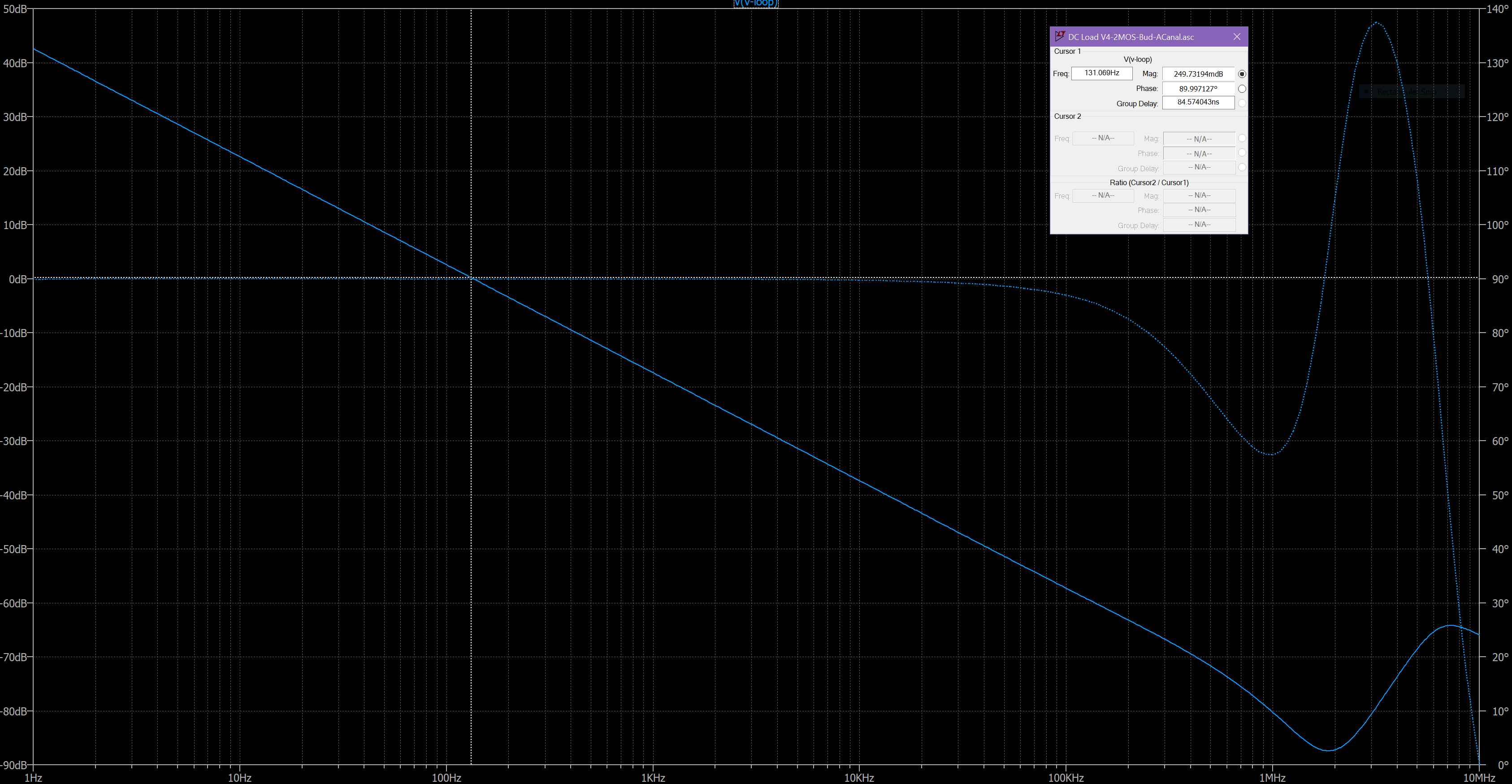
Paul has been working on this for a while. I entered the scene when he had a problem with oscillation that he couldn't explain while evaluating his latest prototype. Paul's blog on this subject is here: https://www.paulvdiyblogs.net/2022/08/dynamic-acdc-load-cc-cv-cw-batt.html
He was attempting to design/build a DC/AC electronic load. I have no need for an AC dynamic electronic load, which is a lot more complicated to design and build, so we settled, temporarily, on a DC version.
A lot of issues have not been entirely addressed yet. There are both hardware and software problems that remain to be addressed, but we're hopeful to overcome them with a bit of persistence.
Project Status (2024-04-25):
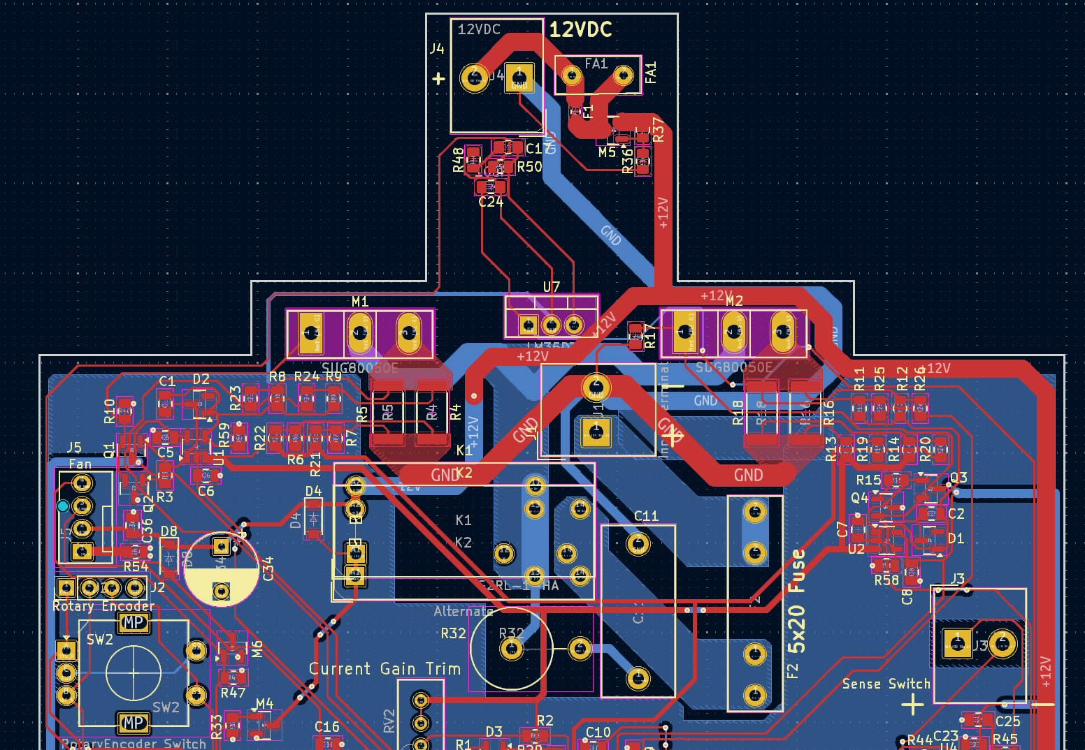
There are problems with the first PCBs.
- We have to put diode isolation between the ESP32 Devkit 5V supply and the Devkit USB interface to prevent large currents from overloading the 12V supply. The Devkit was supposed to have this diode on its board, but instead we found a shorting resistor.
- The voltage sensing circuitry was mis-wired, but easily repaired so we can continue evaluation.
- We didn't realize that the REF5040 required at least a 1uF capacitor on its output for stable operation...WTF?
- The two DACs had SCL and SDA swapped, but the ADC is working fine with the I2C interface.
- The pullups to the ESP32 were all taken to 5V, but should have been 3V3.
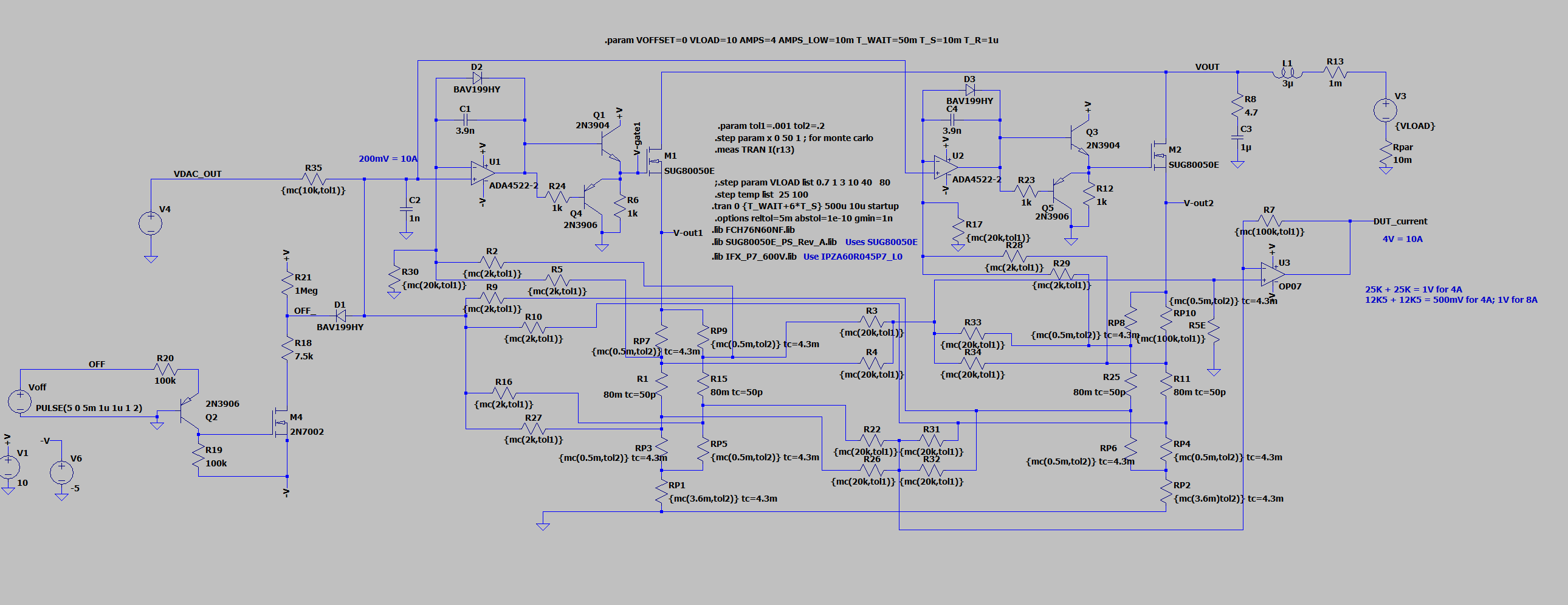
This is all normal stuff and can be easily fixed for the next pass. With changes made to fix the above errors we now are getting current from the load and have calibrated a 1A output to yield 403mV at the DUT_CURRENT signal -- less than 1% overall error. We can store that error and use it when calculating output currents. We have gone to 3A @ 30V, which is the limit of our power source. We're still in the early stages of evaluation, but things are looking good in terms of accuracy and drift.
Paul has the CC, CR and CP modes working in software with good results. The CV mode is a bit iffy and might need to be implemented in hardware.
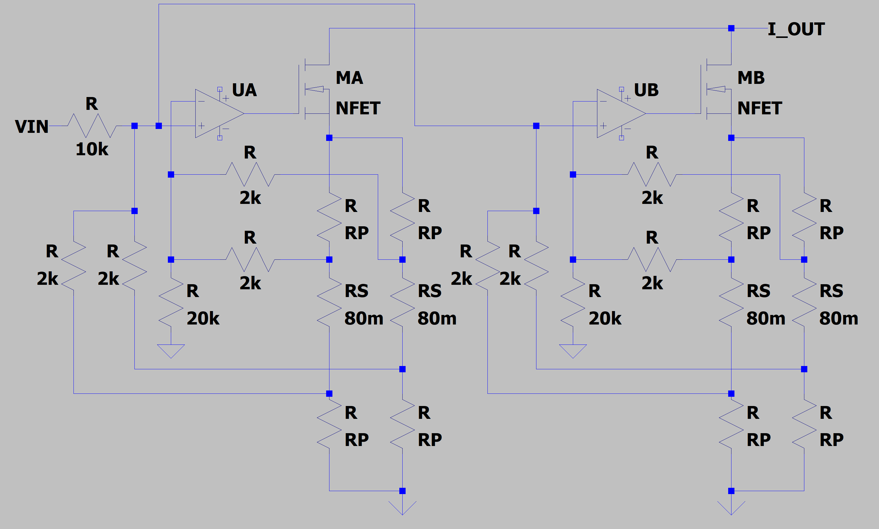
As we proceed in our evaluation we've added a few more features: a Function Generator input for producing arbitrary current waveforms and a current monitoring output for a scope input. The schematic is getting very busy so the feature creep has to stop soon.
We may need a better heatsink and fan because the heatsink is getting hot (71C) with just 30W of continuous power applied.
Target Specs:
Input Voltage: 1V - 100VDC
Input Current: 1mA - 4A for 40V < Vin < 100V, 1mA - 10A for 1V < Vin < 40V.
Maximum Power Dissipation: 150W (Depends upon heatsink and Fan. Bud has doubts.)
Voltage Accuracy: 0.2% (Trimmed, but there are temperature drift terms.)
Current Accuracy: 0.6% (Trimmed. Best guess right now. Mostly temp drift error.)
Lowest Conductance: TBD. (Current...
Read more »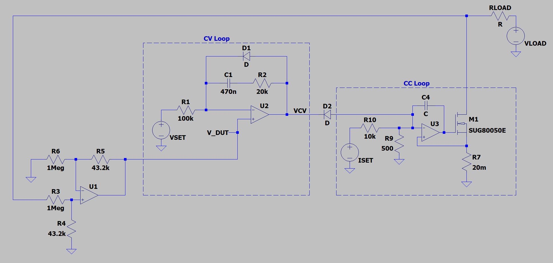
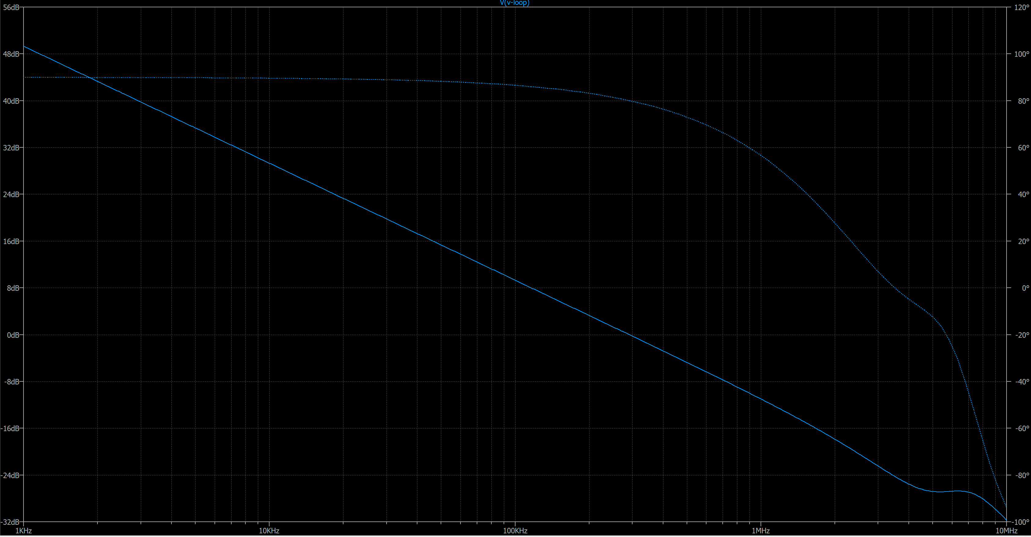
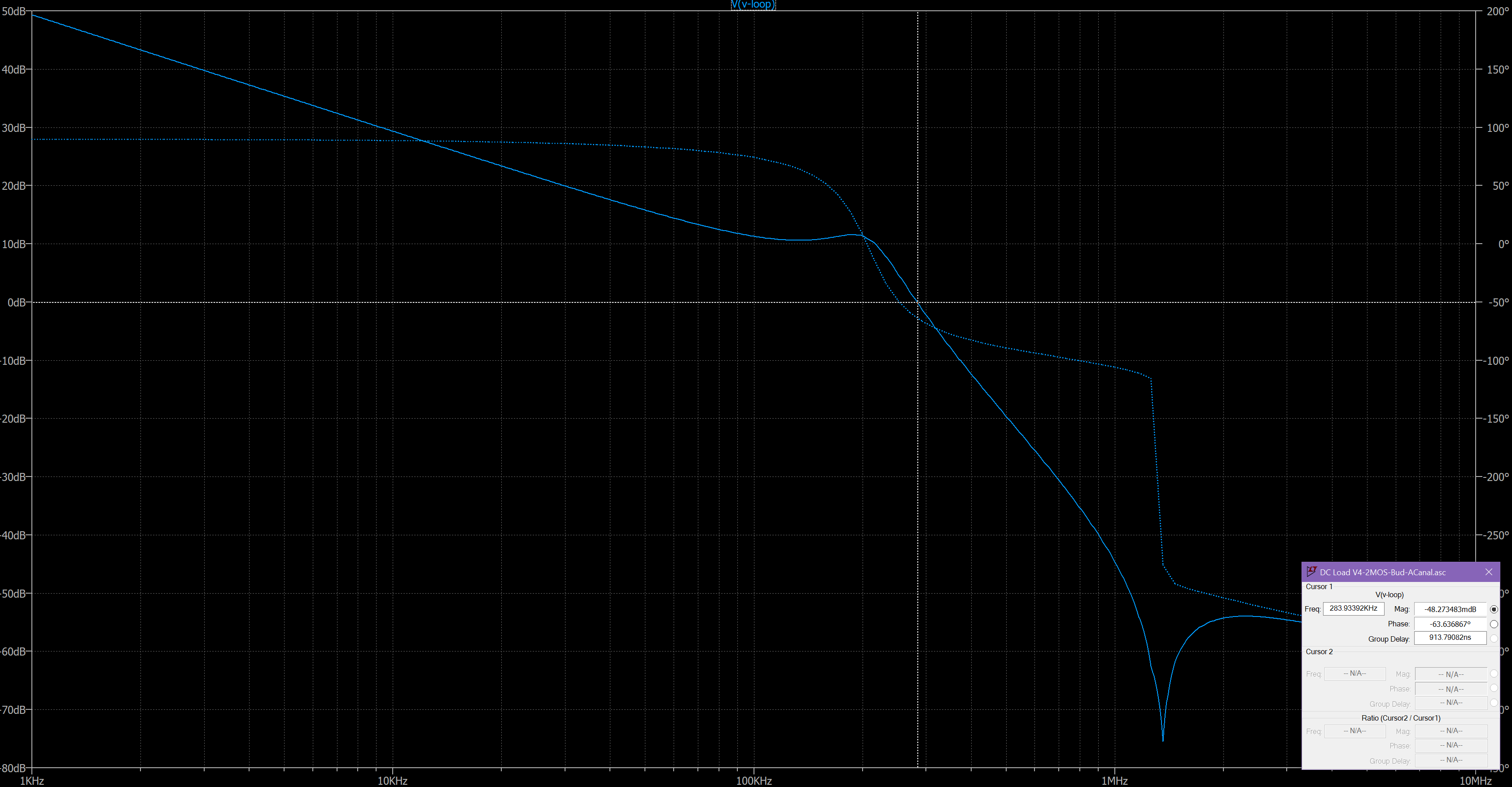
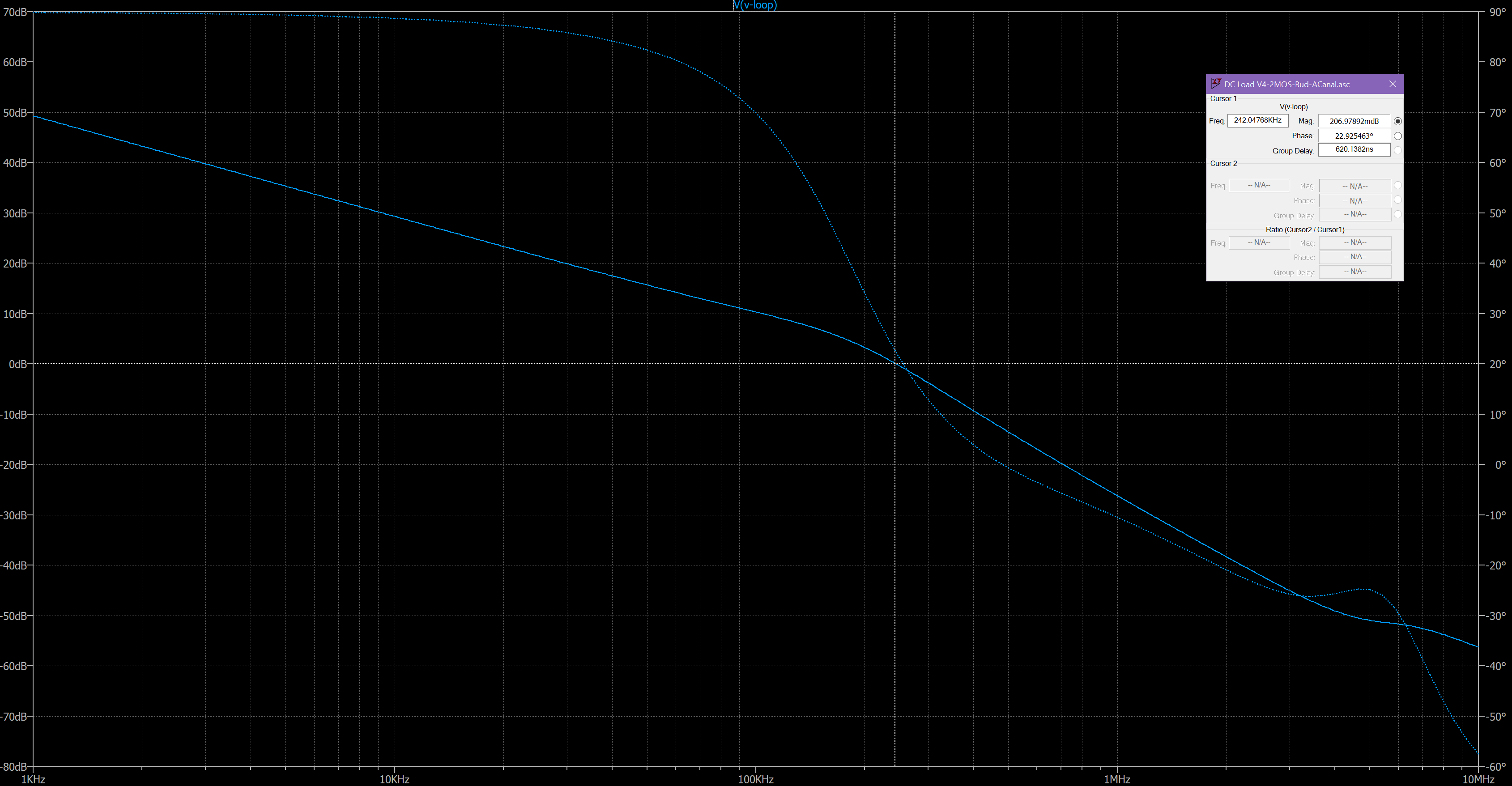
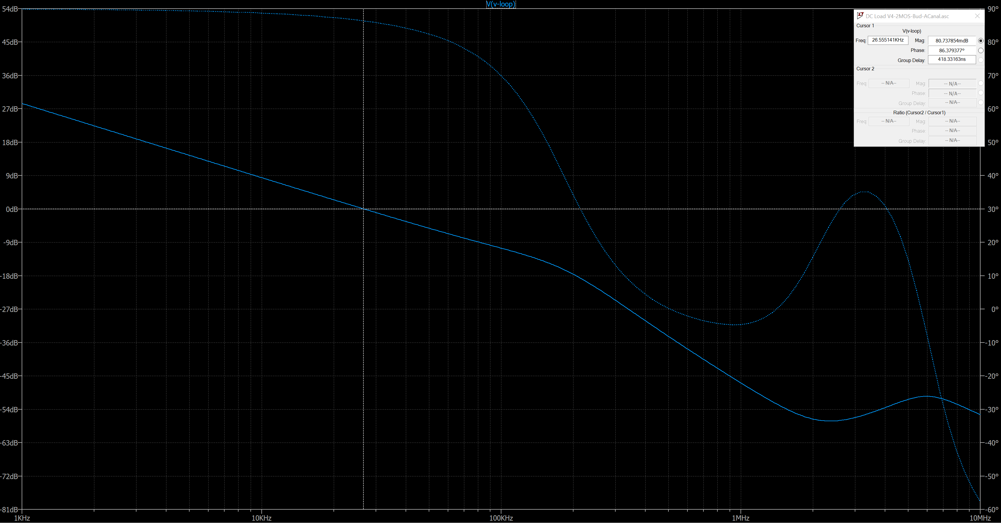
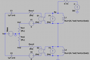
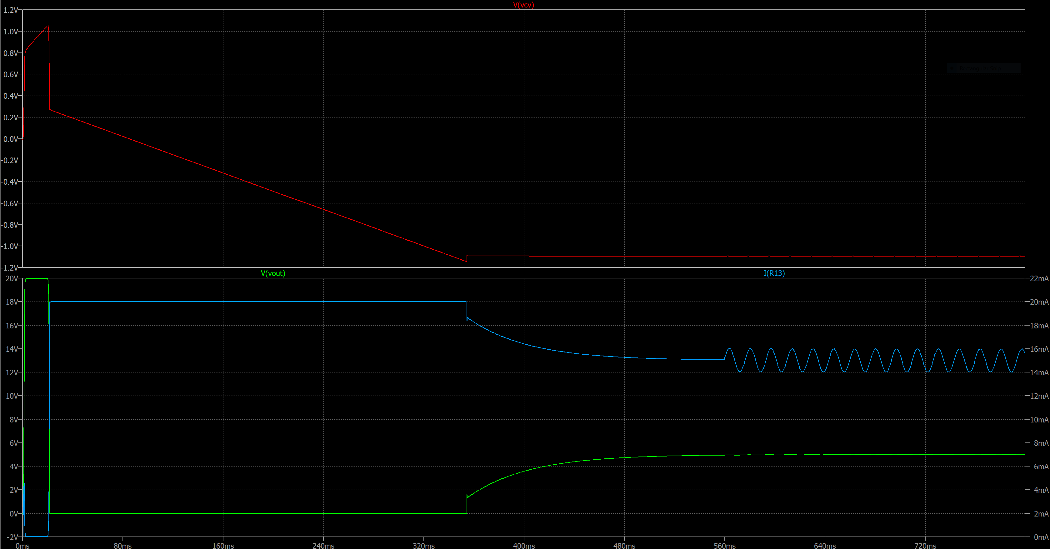 The system is held at zero output current for 5ms and then released. The CV opamp is out of control until VSET changes from zero to 0.2V, but it has to slew to 1.2V below GND before it takes control from the CC loop. Since the CC loop can output 125mA it drives the output voltage to zero (125mA x 1k = 125V, but only 20V is applied). Once the CV loop overcomes the CC loop the current decreases in the CC loop and the load voltage rises to the set point (5V). A 1V-peak sinusoid on top of VLOAD is applied at 560ms to show that the CV loop can keep the output voltage stable when disturbed. I think it performs pretty well, if slowly.
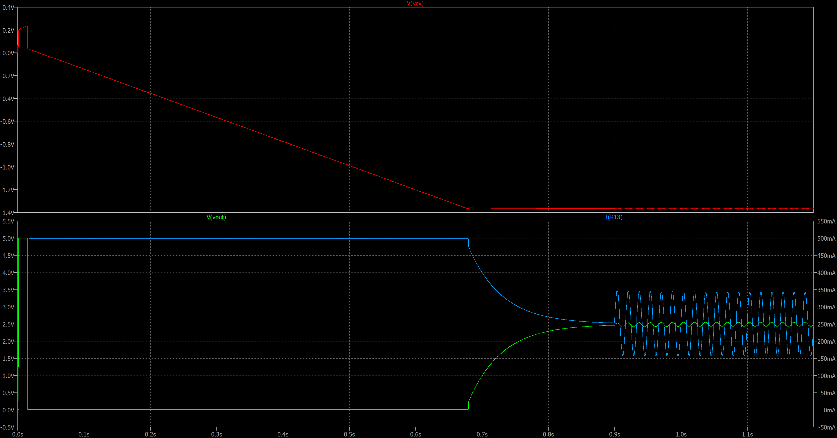
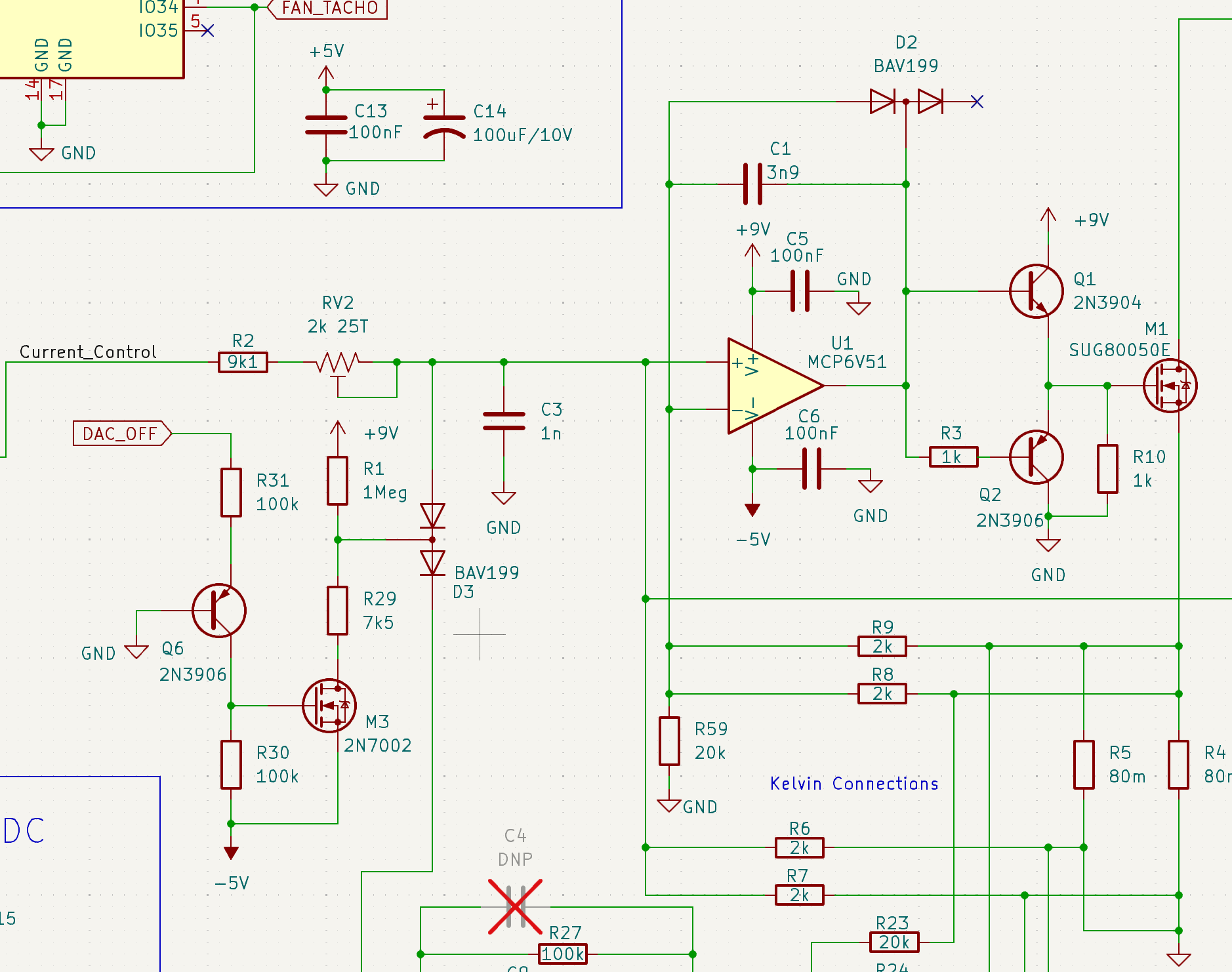
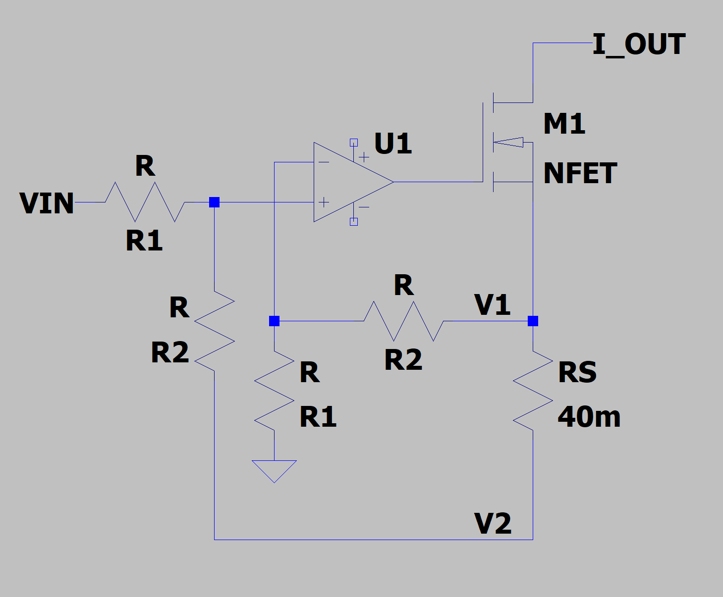
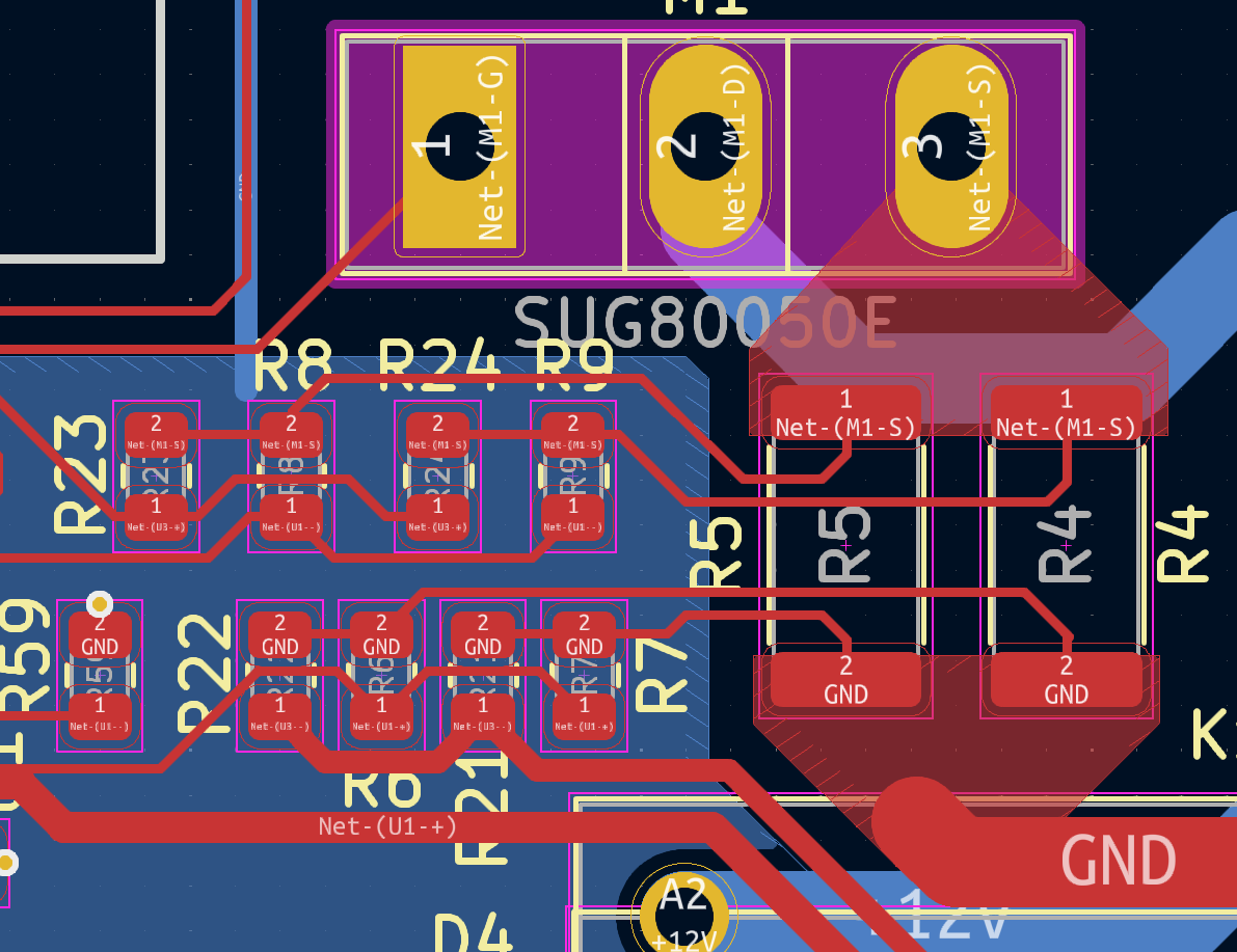 The current tends to spread in 45 degree funnels from a single point to a connection point, such as a pad on a component. In order to make the Kelvin connection the current should be zero at the point of the Kelvin connection. I made triangular copper pours to distribute the current to the two sense resistors. The back-side of the pads should have zero current flowing to it and therefore a good place for a Kelvin pickup. The pickup points are on the middle-inside of the pads on the sense resistors. Those traces connect the feed resistors for sensing the voltage across the sense resistors.
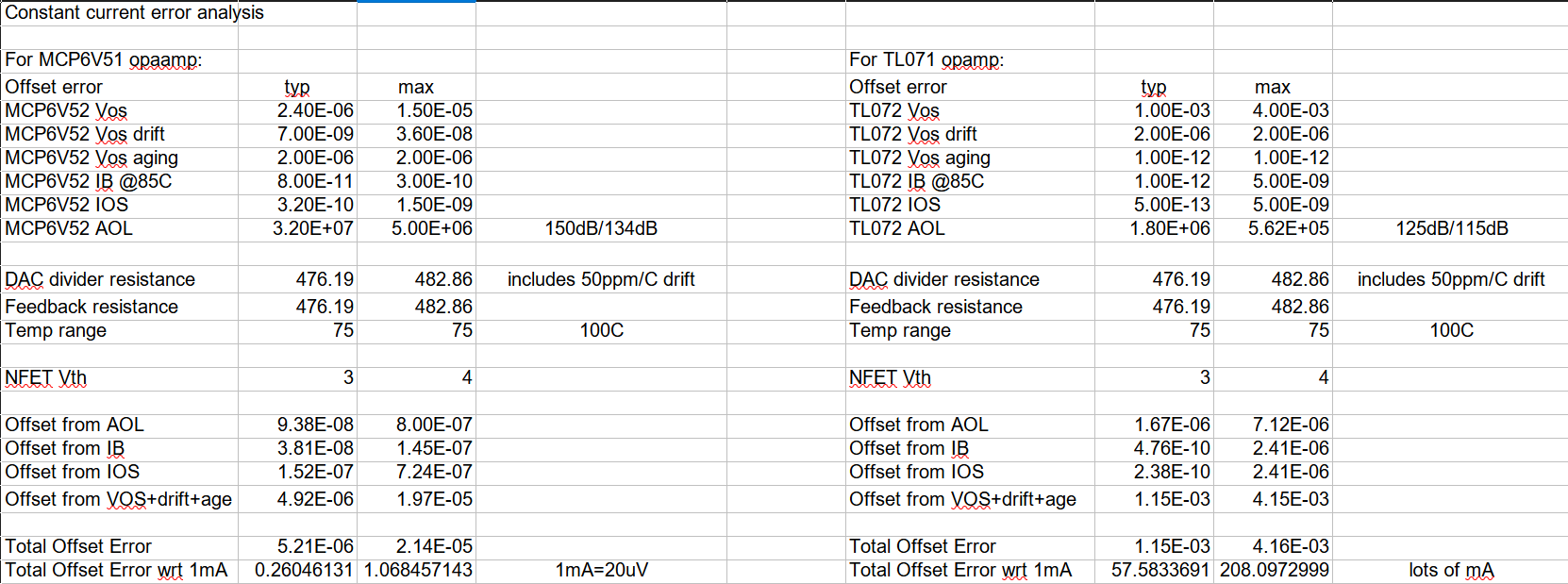


 jbb
jbb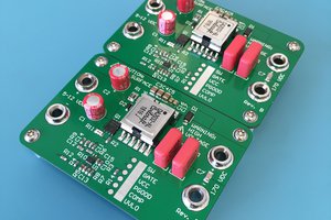
 James Wilson
 Tron9000
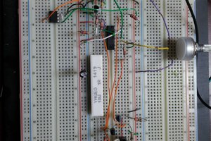
 Marc-O.
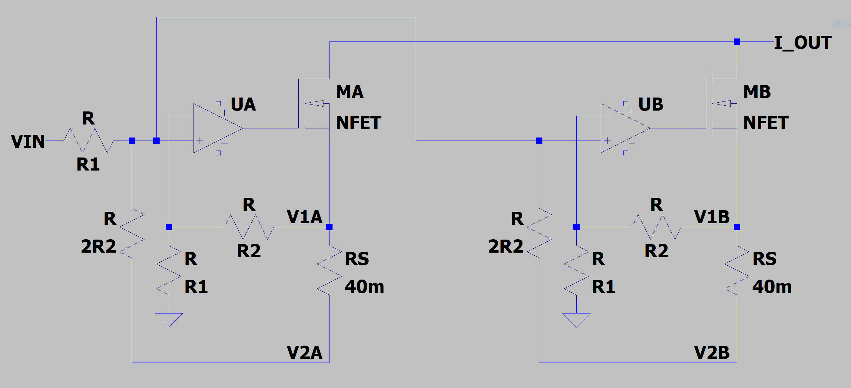
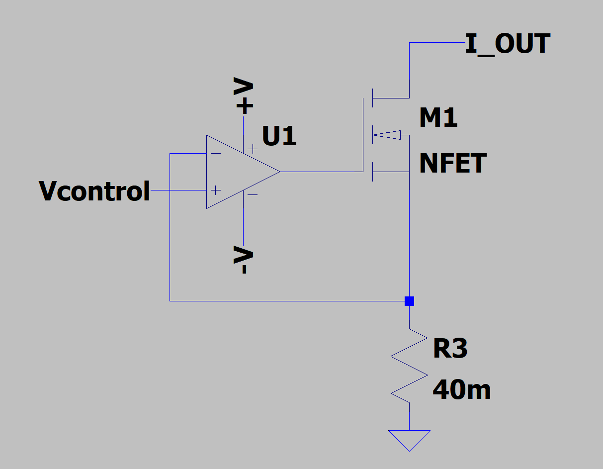
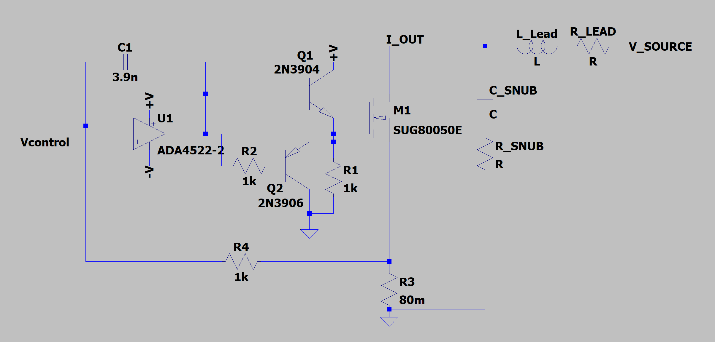
Hi,
Looking at your schematic, I see two completely separate output sections including sense resistors. Is that setup going to load share properly?