 Bud Bennett
After we got the Constant Current (CC) loop stable it was time to account for the configuration of the circuit -- the topology. We stumbled upon a topology that appears to yield very good accuracy with the addition of just a few resistors. This is the basic topology of a single current loop:
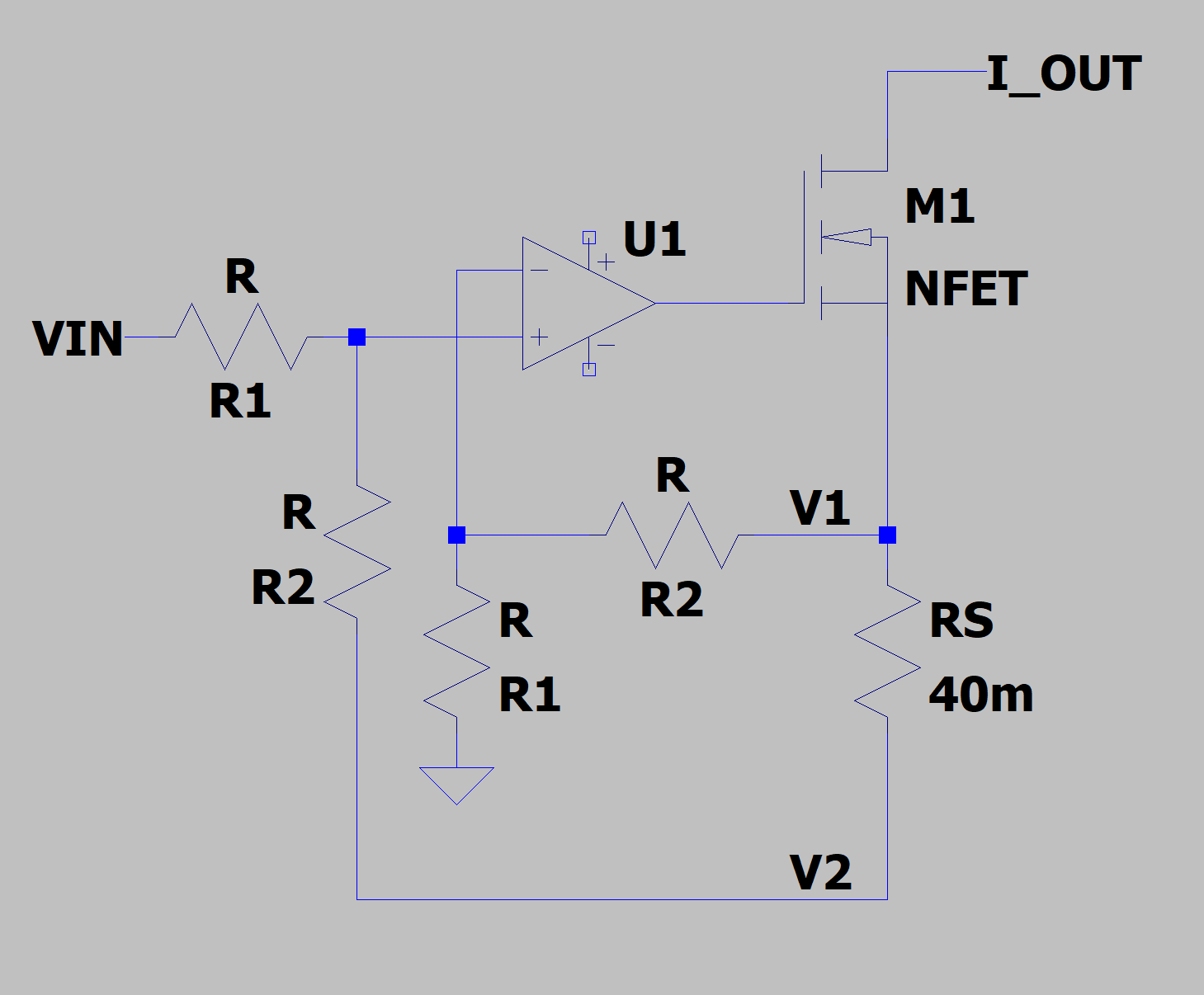
What we need to know is how the output current depends upon the input voltage, VIN. The schematic above uses only 2 values R1 and R2 as a special case of this topology that we employ. V+ and V- are the voltages at the inputs of the ideal opamp (infinite gain, no offset). The equations that govern this are:
V+ = (VIN - V2)(R2/(R1+R2)) + V2
V- = V1(R1/(R1+R2))
Since the opamp forces V+ = V-, when you solve for V1 it yields,
V1 = VIN(R2/R1) + V2 , as you would expect.
And the output current, I_OUT is therefore:
I_OUT = (V1 - V2)/RS = VIN(R2/R1)/RS
Note that V1 and V2 drop out of the equation. Like an instrumentation opamp. The only errors are the ratio of R1/R2 and the value of RS.
When we expand the topology to two separate current loops we get this simplified schematic. Again, the resistors values are special cases to match the topology and make the math easier.
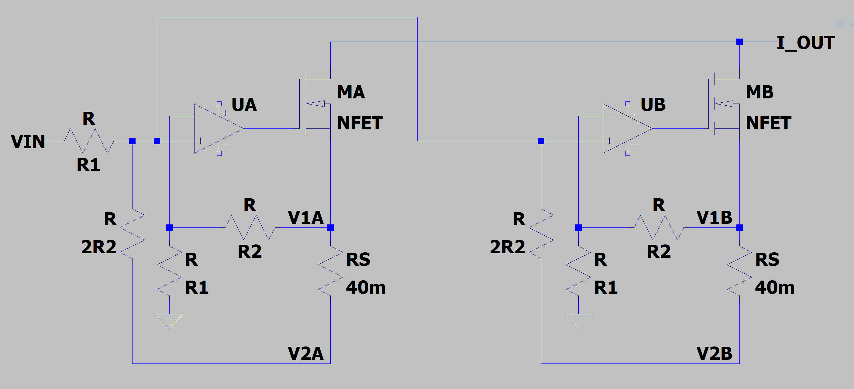
Now it gets a bit more complicated. We want the current, I_OUT, to be only a function of the input voltage, VIN. Here's the equation for V+, which is the same connection for both opamps:
V+ = VIN R1/(R1+R2) + R1/(2(R1+R2)) (V2A+V2B)
and since V+ = V-,
V1A = VIN(R2/R1) + V2A/2 + V2B/2
But what we really need to know is what the output current is:
I_OUT = IA + IB = (V1A - V2A)/RS + (V1B - V2B)/RS
The opamps are forcing V- to equal V+, and therefore V1A = V1B, we can substitute :
I_OUT = IA + IB = (V1A - V2A)/RS + (V1A - V2B)/RS = 2(R2/R1)VIN/RS,
which is only dependent upon VIN and the three fixed resistor values. Of course, this is a trick of a sort since I've forced the resistor values to be identical or 2X multiple. But the errors in the method are below the tolerance of the resistors (sub-1%).
By inspection, it is obvious that if the "B" side of the circuit has errors that increase the current through MB, then a corresponding decrease in current will occur through MA. In order to prevent this disparity from getting too large careful layout symmetry between the two sides must be preserved.
*********************************************
The next step in the process is to expand the sense resistors to two sets of two. This is to keep the power dissipation in the resistors to a reasonable limit. The math gets a bit unreasonable (for me) and so I resorted to LTSpice to corroborate the result -- it is the same.
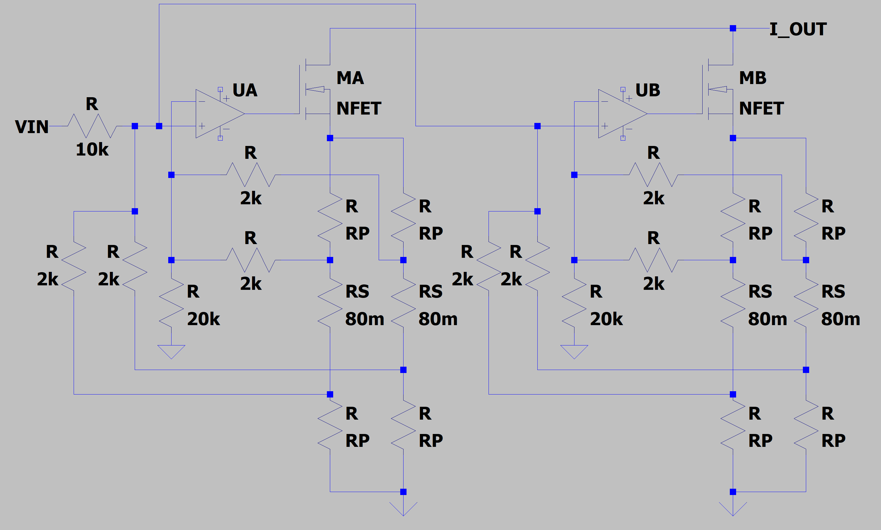
This time I have inserted parasitic resistors, the ones labeled RP, to indicate where the various error voltage will come from. The values of RP depend upon the quality of the PCB layout -- they are not all the same. Note also that the ground return point of the current could be different than the ground reference of Vin. The errors will still be cancelled to a first order. Again, you get the same result, if you keep the resistor values in the same ratios, the output current is only dependent upon VIN, R2/R1 and RS.
**********************
The 2kR resistors must be Kelvin connected across the sense resistor, RS, in order to get the full benefit of this approach.
Simulation Results:
To prove the point I simulated the circuit in LTSpice using monte carlo analysis. Here's the complete circuit:
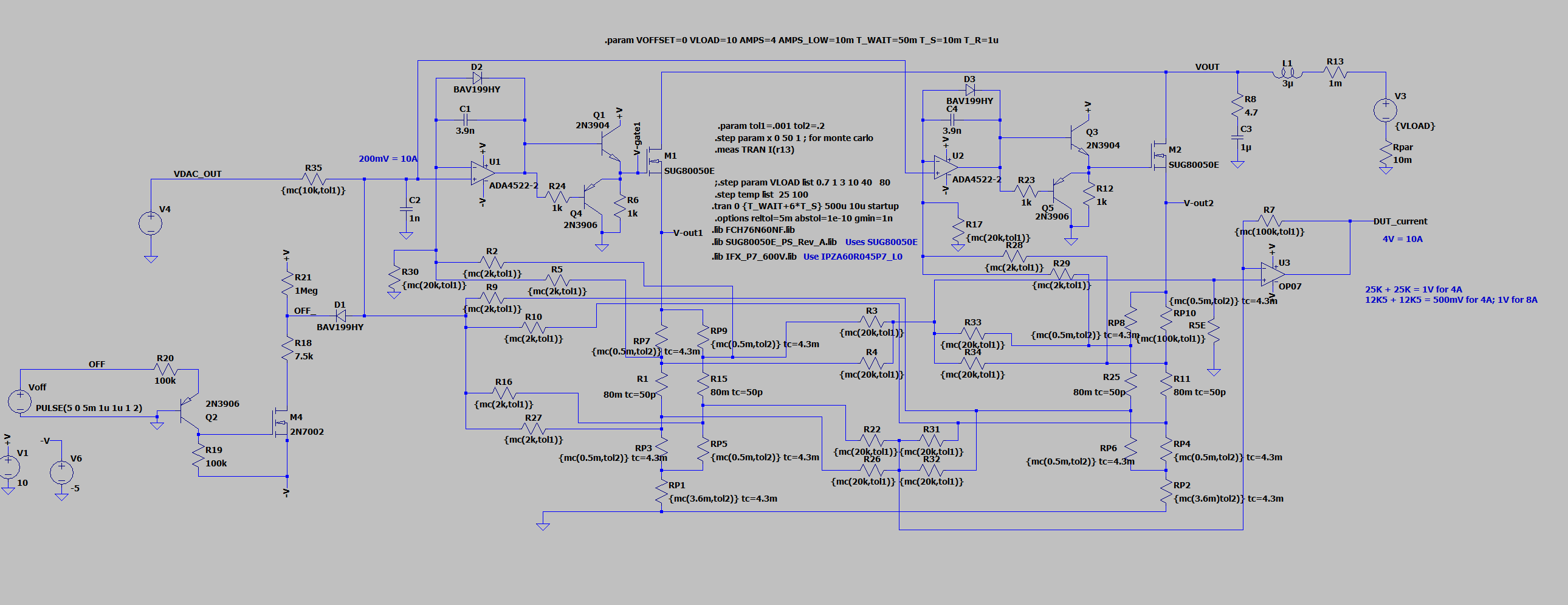
The tolerance of the gain setting resistors is 1%, but I set them to near 0% in the first simulation while letting the parasitic metal trace resistors have a tolerance of 20% and a tempco=4300ppm/C. The siimulation ran 50 times at 25C and 50 times at 100C. The results were uninteresting to say the least -- total variation in output current from the 10A set point was...13.6uA. That doesn't include any opamp variation except temperature. That is a variation of only 0.000136%!
When I added a 1% tolerance to the other resistors the result was more interesting:
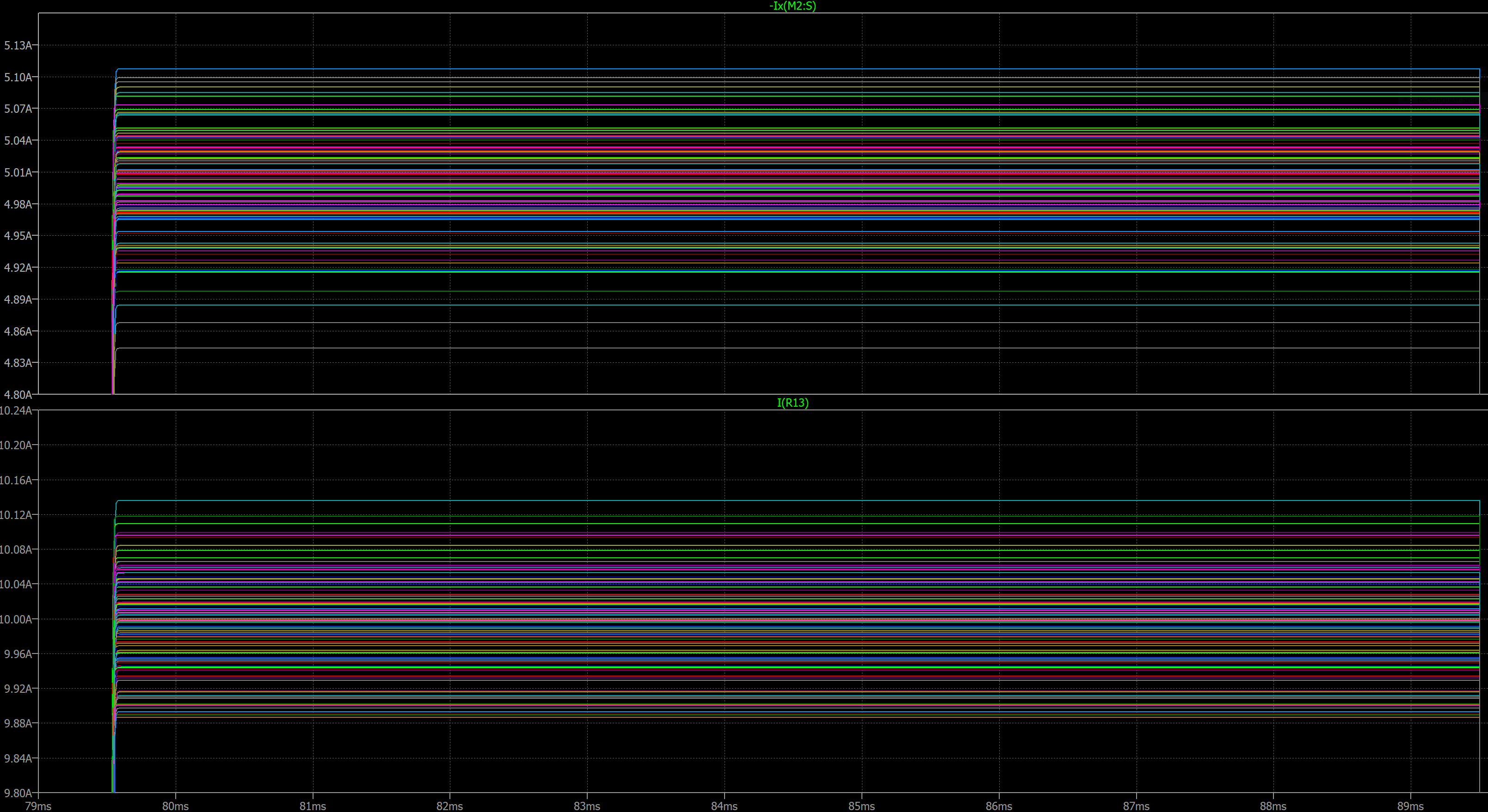 The bottom plot pane is the output current. It varies as expected, about +/- 1.3%. The top plot pane is the current through M2, which varies a lot more due to the 20% tolerance and higher TC that I set for the parasitic resistances. The results get even more interesting when the resistor tolerances are set to 0.1%.
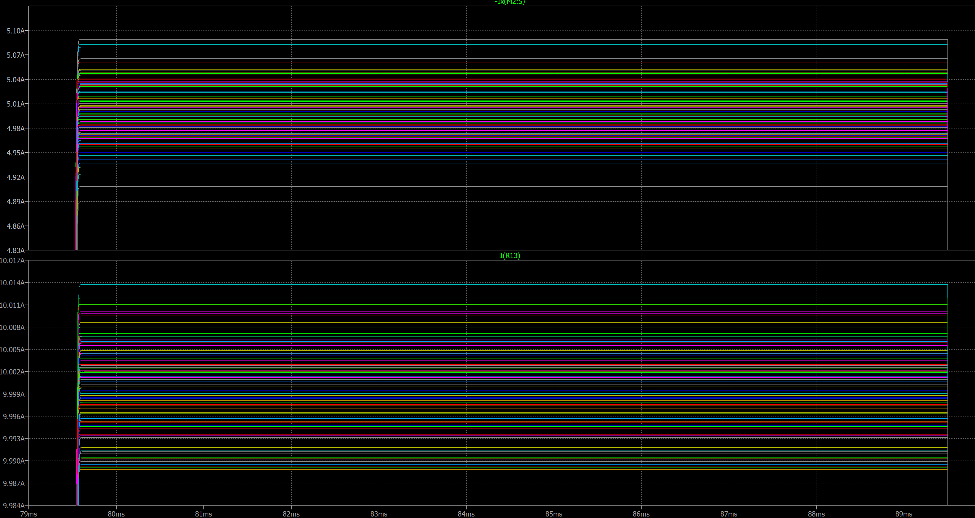
The output current variation drops by a factor of 10, but the variation in the current through M2 doesn't decrease much since it has the added variation of the parasitic trace resistances.
So it would seem that using 0.1% resistors should negate the need for a trim...not so fast. Try to find 80mR 0.1% sense resistors. If you re-run the simulations with 0.1% tolerances for the "regular" resistors and 1% tolerances for the sense resistors the simulations show that the output current variation is 0.62% (not 0.15%). It seems using 0.1% resistors will not yield much better results than 1% overall, unless you can get 0.1% sense resistors (good luck). We're keeping the trim.
Discussions
Become a Hackaday.io Member
Create an account to leave a comment. Already have an account? Log In.