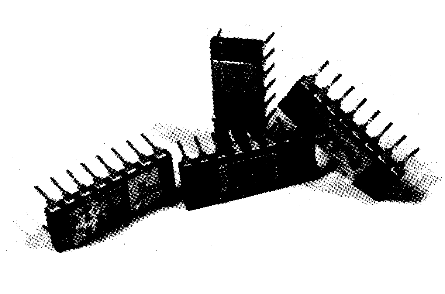
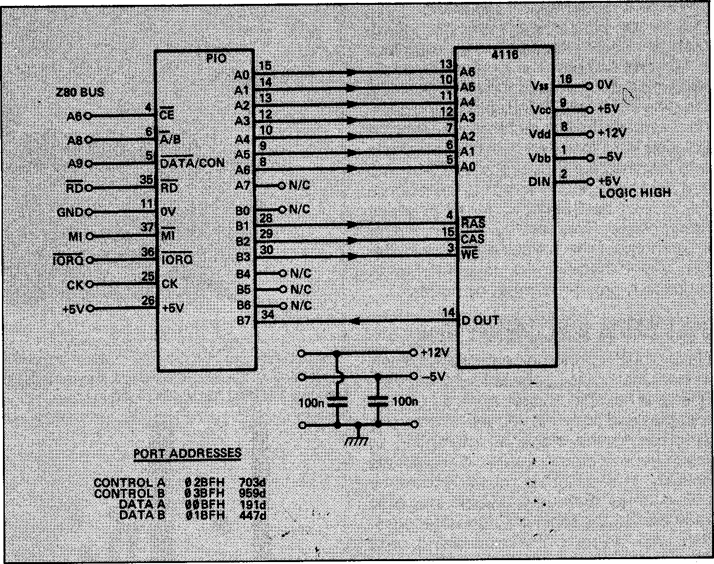
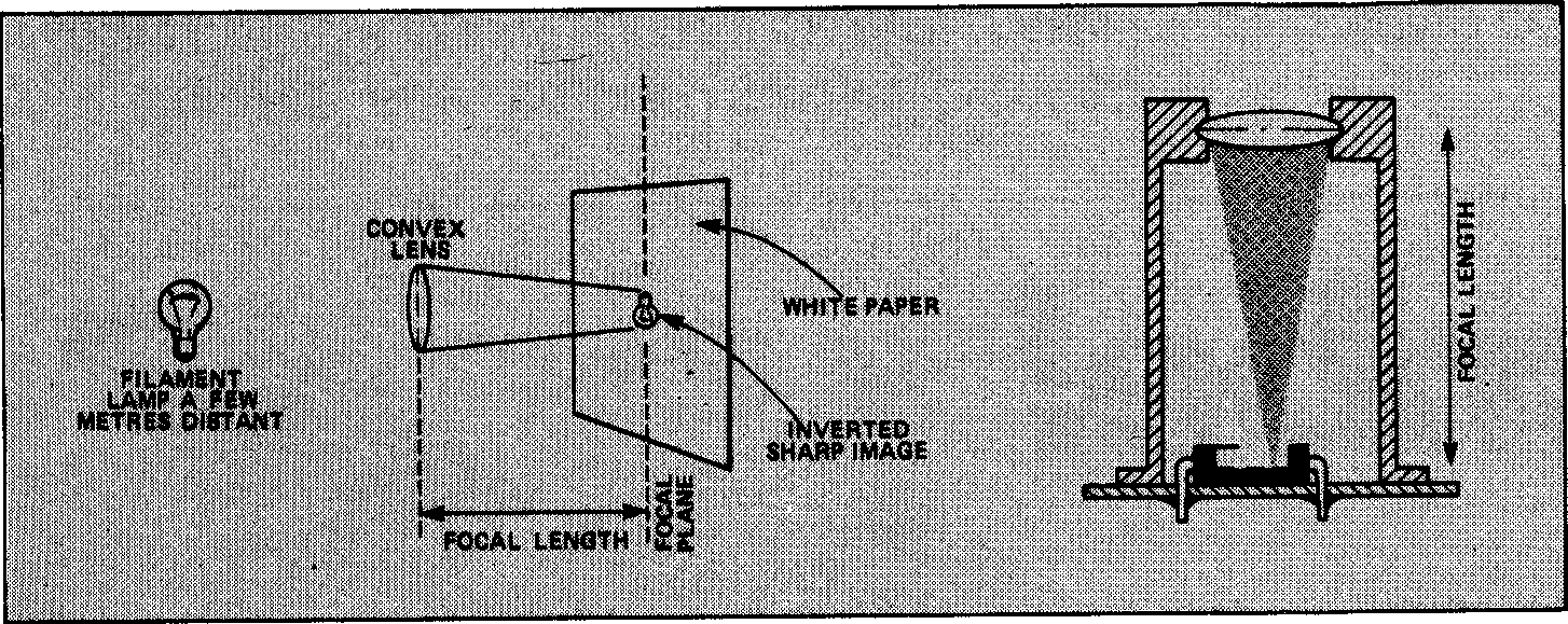
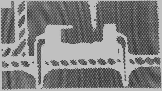
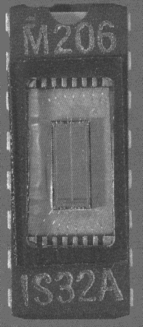
• The Micron Eye

    Keith04/22/2024 at 04:34 0 comments
  • My Printer-port DRAM camera design

    Keith04/22/2024 at 04:12 0 comments

    I have lost the details but I can recall that PD0-7 drove the address lines, the printer control lines drove D, RAS, CAS and WE,  and a printer status line read the data.

    I drove it using my 8088 based Amstrad PC. 

    The cells need time to collect light and discharge, so instead of waiting for a row to discharge I alternately charged a row and read a row that had been charged N rows before. This allowed data to be read as fast as rows could be charged. Varying N adjusted the exposure time. 

    You can't do this with modern PCs because they don't have parallel printer ports and their operating systems would not allow you to directly read and write to I/O space.

  • Byte magazine IS32 camera project

    Keith04/22/2024 at 03:44 0 comments

    This Byte project used the Micron IS32 Optic DRAM, and a serial interface.

    I used the pdf files from here:
    https://archive.org/details/byte-magazine-1983-09/page/n21/mode/1up
    https://archive.org/details/byte-magazine-1983-10/page/n68/mode/1up
    and edited them into a single, smaller file without the adverts here:
    1983_09_BYTE_08-09_and_10_Micro_D-Cam.pdf

  • Your Robot camera project (4116 and Z80 PIO)

    Keith04/21/2024 at 16:15 0 comments

    From Your Robot magazine, April 1984, page 5 onwards

    Taking the tops off 4116 DRAM chips proved to be quite simple, though you should be prepared to "write off" the first one you mutilate. There are a number of things which can go wrong (and did go wrong in the case of our prototypes). However, if you have a steady hand and follow the instructions, then all should be well.

    The design of chip which should be used is the type known as Ceramic Dual-in-line Welded Seal. The pins are side brazed and gold-plated, which although not important, makes the chips easy to recognise. The body of the IC is usually grey in colour and a metal plate is soldered or welded across three-quarters of the top surface. The ICs used in the prototype bore the code HYA4116 A3. The metal plate has to be removed. The first attempt involved using a fine-toothed saw, with the IC already soldered on a piece of Vero board to keep it rigid. This worked, but put fine swarf and foreign bodies. onto the surface of the chip which then had to be blown off. In fact the solder/weld line is so thin that the plate can be cut and prised off using a Stanley-knife and this method produces hardly any loose material. Heating the plate with a soldering iron until it slips off also proved successful. On the exposed chip surface the two rectangular banks of cells making up the memory array can clearly be seen, as can the fine wires connecting the chip terminals to the IC pins. Contamination on the chip should be blown clear. Any brushing is likely to disconnect one or more of the fine wires.

    Having exposed the entire chip surface, the next job is to cover part of it up again. Surrounding the memory matrix are all the address latches, address decoding and buffer gates and if light falls upon them they will fail to control the memory matrix properly! A good lens system would ensure that no stray light endangered the control part of the chip. We tried paint as a covering agent but that was difficult to apply accurately, so in the end the sensitive chip areas were masked off using part of the metal plate. Soldering it back onto the IC resulted in undesirable flux splashes so finally it was glued back.

    A small convex lens was positioned in front of the IC so that the chip surface lay in the focal plane of the lens. Figure 2 shows how to find the focal length of a convex lens. In view of the fact that pieces of cardboard and plastic tape held the "lens,, in front of the "camera", it was perhaps surprising that any images were obtained at all. It will be very interesting to see what standard of results a school science department can achieve.

    Suitable DRAMs can be identified by their packaging and the metal plate, once removed, reveals the capacitor array. The author's initial attempts at chip surgery proved less than successful. 

    Figure 1. The hardware of the Solid State TV camera consists simply of the DRAM image sensor itself and a Z80 PIO.

    Figure 2a (left) shows the method used to determine the focal length of a convex lens. A piece of white paper is moved back and forth until an inverted image of a filament lamp some distance away is brought into sharp focus. The distance between the card and the lens is the focal length. 

    Figure 2b (right) shows the lens mounted such that an image is formed on only one half of the DRAM's capacitor array.

    CONTROLLING THE CAMERA

    The logical arrangement of the memory matrix of any RAM chip can usually be gleaned from its specification sheet. In the case of the 4116 the 16384 memory cells are configured as a 128 x 128 array which implies a nice square area of chip surface to receive the light rays. Unfortunately the physical arrangement of the matrix might not be so convenient since the manufacturers never intended it to be used as a solid state camera! The 4116 is physically separated into two rectangles of 64 x 128 creating a sizeable “blind spot" in the corridor between the two rectangles. In fact the solution...

    Read more »

  • Electronics Today International camera project (IS32 and UART)

    Keith04/21/2024 at 15:55 0 comments

    Image acquisition system

    G. J. AWCOCK, F. W. STONE AND R. THOMAS

    A low-cost solid-state sensor, coupled with suitable image-processing software, is more than adequate for many applications in robotics, security and character recognition.

    Fig. 1 (above). Raw image acquired by the IS32 sensor: the picture shows light falling on another IS32.

    Fig. 2. Micron Technology's IS32 optic DRAM: a 64K memory device with a transparent lid. Price is about £40.

    In many cases the broadcast TV format is selected as the basis of an image processing system for no better reason than its familiarity, or ease of display on standard monitors. However, the quantity of data required to represent a high-resolution image is a major factor contributing to the inaccessibility of computer vision; and so it is essential that very careful consideration of the system requirements should result in a sensor specification which is adequate, and no more.

    A conventional TV camera produces an analogue video signal which is continuous in the horizontal axis but discrete in the vertical axis, by virtue of the raster scan method of picture reconstruction. The maximum re-solution in the vertical axis is approximately 574 lines, with interlace, and because the horizontal:vertical aspect ratio of a standard TV screen is 4:3 this implies a horizontal resolution of approximately 765 picture elements (pels, or pixels). Thus the number of pixels required to represent a full-resolution picture is 574 × 765 = 439,110.

    If, in addition, each pixel is represented as one of 64 grey levels, i.e. a grey-scale resolution of six bits, the quantity of data which must be acquired for each picture will be a grand total of 2,634,660 bits for a monochrome signal! Thus the scale of the problem of acquiring images and storing them in a personal computer becomes obvious.

    In addition, a new picture is generated every 40 ms, leading to a throughput requirement which makes real-time camera/ computer interfaces both complex and costly. This problem has been tackled to some extent for static or slowly changing images by the development of slower multi-frame TV interfaces, which build up their images over a number of consecutive frames. This eliminates the problem of video-rate a-to-d conversion and considerably reduces the cost of an interface, but it does nothing to ease the problem of storing this quantity of data within the computer.

    Solid-state image sensors should offer hope of a simpler interface, since the data is inherently discrete in both the horizontal and vertical axes. Generating distortion-free raster scan video is then a relatively simple problem for digital electronics.

    Unfortunately, the best known of solid-state sensors, the charge-coupled device (CCD), does not have many advantages over conventional vacuum tube cameras in low-cost applications.

    In general, CCDs have been designed with the full TV standard specification in mind, offering spatial resolution of typically 380 × 488 pixels with continuous grey-scale dynamic range of typically 1000:1. Thus they do very little to ease the problem of excessive image data; and a sensor free of blemished photosites (i.e. light-sensitive cells that are defective in some way) costs considerably more than a complete normal TV camera.

    There is, however, a relatively new solid-state image sensor which is ideally suited to experiments with computer vision. The device is the IS32 optic DRAM (Fig. 2) from Micron Technology, which is based upon a 64K dynamic ram and thus offers 65 536 pixels, each having a one-bit grey-scale. The pixels are organised into two banks of 128 × 256, separated by a thin dead-zone, which effectively makes one of the banks redundant for use with normal optical systems. Hence the working resolution of the device is 128 × 256, making it well suited to the high-resolution screen modes of many popular computers. The one-bit grey-scale maps well on to the limited range of colours...

    Read more »

  • Cromenco camera project

    Keith04/21/2024 at 15:55 0 comments

    The Cromenco camera project is already well documented on Wikipedia.

  • Basic theory and previous designs

    Keith04/21/2024 at 14:26 0 comments

    Dynamic RAM cells store electrons which can be knocked out their capacitors by photons. They can thus be used as simple photo-sensors. Light can also interfere with the rest of a DRAM chip. 

    There are several designs based on this idea. 

    • The Cromemco Cyclops, circa 1975, used lots of TTL to drive the chip and produce an image that could be viewed on an oscilloscope. The computer interface was S100 and the code was in 8080 assembler.
    • A company called Idetix produced a slightly modified DRAM with metal layers to shield the part of the DRAM where light-sensitivity would cause malfunctions. Their design used lots of TTL and interfaced to the 6502-based Apple.
    • Electronics Today International produced a 4164-based design interfaced to the IBM PC ISA bus, and used lots of TTL.
    • Your Robot magazine produced a design interfaced to the Sinclair Spectrum bus. It used a Z80 PIO and a 4116 chip which required -5V and +12V rails.

    I had moved on to the IBM PC by this time, but did not want to wire up the E&WW magazine design and put it into my Amstrad PC. I had the idea of driving the DRAM chip with the parallel I/O of my printer port. Obviously software is slower than hardware, but this was never going to be a high-performance camera.

    I got my design detecting light and dark, with a 'moving shutter' method reading rows while waiting for other rows to discharge. However, the pixel pattern did not match the E&WW design logic. I did not have the time or motivation to find the correct unscrambling, as I felt I had proved the principle.