Thomas
-
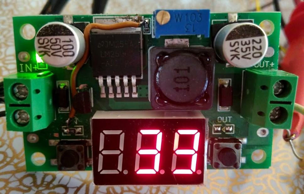
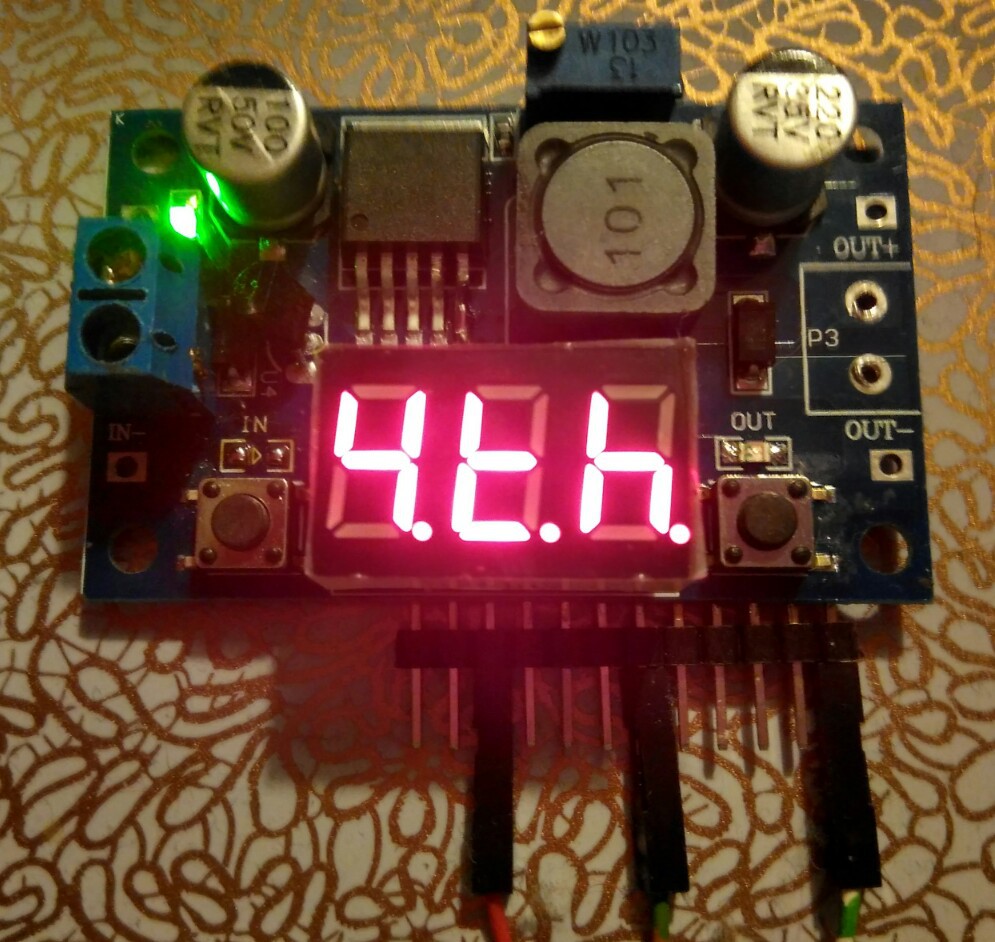
Switched load test with a modified DC-DC converter
03/11/2017 at 16:49 • 0 commentsI modified one of the new "green" DCDC converters along the lines of the solution for a LM2596 based variable DC/DC converter proposed by @K.C. Lee:
- LEDs "IN" and "OUT" removed
- 47R 0804 added instead of LED "IN" (PC.3)
- Trace from LM2596 heat sink/GND to 330R in feedback loop cut, C 10µF 0603 added
- Trace from +3.1V to LED "IN" anode cut, 3mm solder mask on trace removed
- wire from 47R to 330R in feedback loop added
This modification replaces the GND of the LM2596 feedback input voltage divider with a variable voltage, controlled by a PWM output of the voltmeter's STM8S003F3P6. The LM2596 compares the feedback voltage with a reference voltage of about 1.25V, and thus adding a bias voltage to the feedback reduces the output voltage of the DC/DC converter
![]()
Additional changes were:
- 10µF added to the LM317 (back side)
- 0.1µF added to STM8S003F3P6 pin 7 Vss (back side)
- Firmware DCDC flashed (branch develop)
With the new firmware, it's possible to establish a half-duplex console session via PC.7 (pin3, DP of the LED display) using a diode (anode PC.7-RxD, cathode TxD). While the session is active, the DP (decimal point) of the 7-LED display remains inactive.
![]()
With the Forth script from one of the previous posts, the STM8S main Timer(TIM1) reload value is 1000, and at 16Mhz clock the reload period of TIM1 is T=62.5µs.
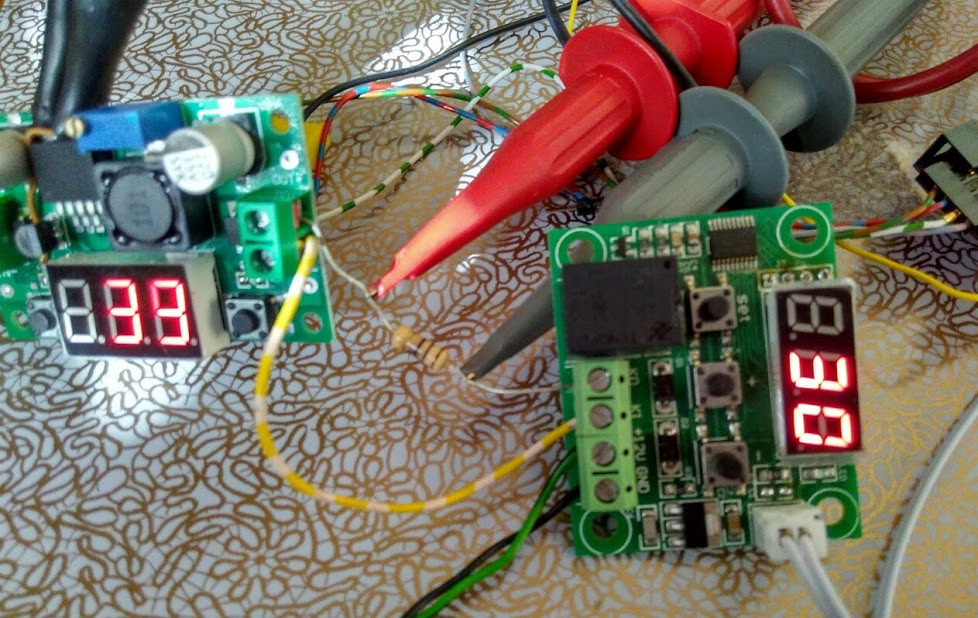
For calibration, the output voltage of the DC/DC converter was adjusted to 13V with the trimmer, while the PWM duty cycle was set to 0. The power supply I used is a land-fill grade "wall wart" (i.e. transformer, bridge rectifier, C 470µF, output voltage about 16V), which means that the results can be expected to be on the pessimistic side.
The RC filter used for converting the PWM signal to DC has τ= 47R * 10µF = 470µs. With T/τ= 7.5 the passive filter appears to be sufficient for our needs (33R, or 4.7µF should work, too).
On the serial console, the command line "330 pwm" sets a duty cycle of 33%, which results in a DC/DC converter output voltage of about 3.3V (which is pure coincidence). In order to test the transient response I used a W1209 as a variable pulse generator (10 lines of Forth, including UI, hacked in about 10 minutes, about 30 lines after "beautification"). The NO contact of the W1209 contact switches a resistor of 18R as a variable load.
![]()
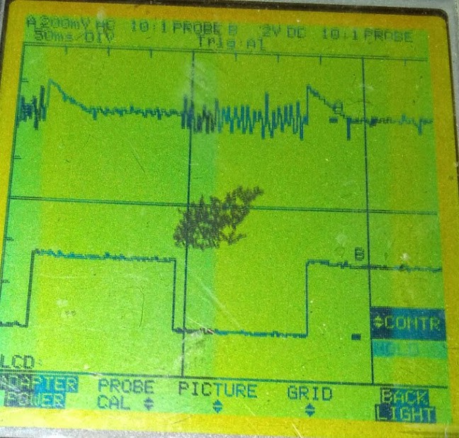
My trusty old scope (an almost 25 years old Fluke Scopemeter with damaged LCD) reads both the output voltage of the CN2596-2 (AC, 200mV/DIV), and the switched GND of the load resistor. The result isn't pretty. There is an overshoot of 200mV when the load is removed, and the noise under load is quite high (also about 200mV).
![]()
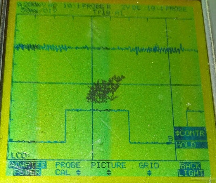
For comparison, I repeated the test with an unmodified "green" CN2596-2 adjusted to 3.3V. As expected, both noise, and transient response are much better.
![]()
The reason for the much poorer performance is the GND offset of about 1V (33% PWM) in the feedback loop, which forces the output voltage down from 13V to 3.3V. This was expected, as feedback loop amplification is now just about 20% of what it used to be: (1.25V - 1V) / 1.25V = 0.2.
Whether the control performance is good enough, or not, depends on the application. However, the setup represents almost a worst-case situation. If the at 0% PWM the feedback would have been adjusted to a lower value (e.g. 7V), or if the PWM duty cycle would be lower (e.g. 20% PWM for about 9V output voltage), the resulting feedback loop amplification, and therefor noise and transient response, would have been better. In any case, this setup is appears to be sufficient for test automation (especially e.g. brown-out, and bad/noisy power supply simulation).
Level up :-)
-
Still problems with serial port and 7S-Display [solved]
03/04/2017 at 19:54 • 0 comments,It's been a while since the last update. My last experiments with the blue CN2596 boards revealed a problem with the reliability of the simulated serial interface when less than 3 digits of the LED display were active. The old board suffered some "bad stress", and there was at least a tiny chance that the problem had to do with that.
I now received a couple of revised DCDC boards with green PCBs marked CN2596-2. The new boards have unpopulated pads for a ICP connector (Vss, SWIM, NRST, GND), and I retrofitted a pin header to it. After flashing the DCDC code it showed exactly the same behavior as the blue DCDC board.
It must have something to do with the PC.7 interrupt, and I still hope that it's a bug in the 7S multiplex code, and that it has nothing to do with the lack of capacitors in the power supply, or current limiting resistors for the LED display.
By the way, the parent project made some good progress.
EDIT1: unfortunately it has something to do with the 7S-LED display. When I remove it (on the blue board it's socketed) the display contents doesn't influence the serial communication at all. When I plug it back in, the communication problems appear. I'm now looking for a workaround.
EDIT2: actually it's a no-brainer: the communication through PC7, which normally drives the DP segment, works if at least 2 other segments are lit (then the port sinking the common anode limits the current sufficiently). Sorry, no sign (-) while the communication is active. For a power supply that's easy.
EDIT3: I hacked the LED MPX routine to mitigate the handicaps inflicted by the abysmal design. Of course, it would be safest to disable the LED display, but no risk no fun, right? -
CN25960-2: ICP pads on the back of the PCB
02/22/2017 at 18:33 • 0 commentsToday I received 3 more DC/DC converters marked CN2596-2 which are similar to the one described before. Visible differences are the pads for a ICP (in circuit programming) header on the back of the PCB, and that they're green.
Although the PCB was redesigned, but it doesn't look like the more obvious shortcomings (no current limiting resistors for LEDs, keys share port with 7S-LED, no blocking capacitor for VCC) have been improved (but I'll open one to be sure).
In order to make modding one easy, I'll try to modify the boards with a few simple steps.
-
First results for "variable output voltage"
02/08/2017 at 21:56 • 3 commentsThe approach proposed by @K.C. Lee seems to be working: using the Forth snippet from the last log entry and a quick&dirty RC filter I can control the output voltage of the DC/DC converter even if the current filter output leaves a lot to wish for.
With an unregulated 12V power supply from the AR-box *), 0% PWM results in 14V output voltage. The output voltage drops to about 2V at 50% PWM. The RPM of a connected DC motor can be controlled in small increments by changing the PWM value (I know, for a motor a constant voltage supply and a PWM output would have been just as good - the motor was just a load for a test).
All in all it looks promising, but I first need to build a set-up for testing. For this I need a switchable load to do basic dynamic testing, a more reliable primary power supply, and good wiring.
*) thanks to @esot.ericor this "croponym"
-
Some progress, and a refresh of a lesson-learned
02/05/2017 at 12:40 • 6 commentsIn the last log I listed some ways for controlling the output voltage of the LM2596 with a limited modification of the CN2596-2 DC/DC module, which I found challenging. The challenge was accepted and won by @K.C. Lee: it's easiest to add an offset to the ground of the feedback voltage divider!
The idea is to create an offset voltage between 0 and 1.2V and thus change the behavior of the feedback. This way the LM2596 "native" feedback loop retains at least some of the closed loop control, and an overlay PI control loop can do the rest.
The offset voltage can be produced with a PWM signal and a simple RC, but it took me some time to figure out how to configure PC3 (TIM1_CC3) as a PWM output (hint: it's a bit more complicated than configuring TIM2 for PWM, and there is a red herring in the manual).
With the help of a small Forth program the concept can be tested:
file
: iTim1 ( n -- )
  tim1_arrh 2c!
  1 tim1_ccer2 c!
  $80 tim1_bkr c!
  $60 tim1_ccmr3 c!
  1 tim1_cr1 c! ;
: pwm ( n -- )
  tim1_ccr3h 2c! ;
: vOut ( -- )
  4 adc! adc@ 100 184 */ . ;
' vOut bg !
1000 iTim1
300 pwm
hand
iTim1 initializes TIMER1 with the reload value "n", and configures TIM1_CC3 as a PWM output.
pwm sets the compare value to n.
vOut reads Ain4, scales it by a factor of 1/1.84 using */ for 32/16 bit arithmetics, and displays the output voltage in units of 100mV.
The value is shown on the LED display because it's set as the background task with ' and bg !. The timer is then initialized to 16kHz, and the PWM duty cycle is set to 30%.
Please note that the whole program is just 13 lines, 51 words, or 215 characters long. It compiles to 93 bytes of code, and it doesn't require any variables since all intermediate values are passed through the Data Stack of the Forth VM.
I rectified the PWM signal from PC3 with a simple RC filter, and connected it to the voltage divider. It worked nicely, until I decided to enable the LM2596. When I then saw a negative voltage of about -13V at the capacitor I immediately knew that I should have spent more time drawing the schematics of the board, and less hacking the software. PC3 seems to be retired now.
Until I find a way to replace the µC on the board (or the new boards arrive), I'll be using a STM8S003F3P6 breakout board, with a pair of 1N4148 diodes for protection, which I should have done from the start.
A lesson-learned re-learned :-)
EDIT: a second examination of the board shows a normal PWM output. My breadboard wiring must have fooled me. I corrected my error, and also fitted two 1N4148 to my experimenting DC/DC board.
-
The LM2596 "variable output voltage" challenge
02/03/2017 at 18:02 • 8 commentsControlling the LM2596 with minimal modification of the DCDC board is the main challenge. The most obvious way to do this is by manipulating the LM2596 feedback input with PC.3. Setting two different voltage levels is simple, and it has already been demonstrated.
The next level is closed loop control of the output voltage within a certain range.
The adjustable variant of the LM2596 (the one used in cheap boards) compares the feedback signal with a fixed reference voltage of about 1.23V (1.18V to 1.28V through the temperature range) using a fixed voltage divider, and sets the converter duty cycle accordingly
Variable controlling of the output voltage requires the following elements:
A) Reading the output voltage can be done by either 1) reading the output voltage, by 2) reading the feedback voltage, or 3) with a combination of the two.
B) Controlling the output voltage with the STM8 can be done by 1) setting the feedback voltage, by 2) changing the feedback ratio, or 3) with a combination of the two.
The B3603 (refer to HaD Power Supply B3603 Alternative Firmware) uses method A1-B1.
I want to try A2-B2, A3-B2, or even A3-B3.
Here is how:
- The DCDC board has a low pass filtered measurement of voltage "Vout" which limits the control amplification P. It would be usable for "slow but accurate" I control.
- Fast feedback measurement can be done by "unfiltered" conversion with PC.3 if the conversion is synchronized with the LM2596 150KHz oscillator. Gain is likely limited by the acceptable noise.
- Using the native feedback loop of the LM2596 would allow much better control performance, but this requires a sufficiently variable voltage divider controlled by the µC (two levels is trivial)
- Controlling the feedback ration might be possible by controlling the voltage divider switch duty cycle with PC.3 PWM. If this works depends on the behavior of the LM2596.
- Using a small capacitor in the feedback loop, similar to what's described in LM2596 datasheets, might create a "B3 property".
Synchronization and control is possible with the help of Timer1:
- TIM1 can do up to 107 ticks in one oscillator cycle
- ADC conversion can be linked to a TIM1 compare with TRGO
- closing the control loop by setting the PC.3 "feedback duty cycle" can be done in a TIM1 overflow (or compare) interrupt
Open questions are:
- whether the LM2596 remains stable with such a kind of "bending"
- how can TIM1 be synchronized with the LM2596 oscillator without using an additional GPIO
Suggestions, or feedback, are welcome!
-
First code on GitHub, and the limits of circuit bending [solved]
01/31/2017 at 06:27 • 4 commentsThe first working code is now on the GitHub develop branch.
The following features work:
- communication through PC.7 (LED display pin 3, segment DP)
- SWIM-programming-without-NRST through PD1 (LED display pin 4, segment C)
- 7-LED display with 1/8 MPX (hack for lower duty-cycle)
- controlling the LM2596 with PC.3 and PB.4
- Vin/Vout voltage measurement with ADC! and ADC@
When testing the code I noticed that the serial connection isn't always working reliably when I use the on-board LM317 power supply. I'll have to test if that's because of the very hacky Chinese-expert LED control without current limiting resistors, the "innovative" economization on the use of capacitors, or because of the rather poorly defined voltage threshold of the likewise Chinese CH340 USB-Serial chip I use for the very very hacky German single wire serial console in combination with all of the above.
I'll update this post as soon as I know the cause of the problem.
EDIT1: I tried an ARK3116 USB serial adapter: much better, very much better. Looking for that 10 years old mobile phone data cable in the basement is time well spent.
Lesson learned: if it works with a CH340 it works with about anything. If it doesn't work this doesn't mean much ;-)
EDIT2: the scope picture of my "multiplexed" serial interface doesn't look good: most likely I'm doing something wrong when changing the GPIO properties during LED MPX (which the CH340 isn't robust enough to handle). This will have to wait a bit, since for the next days I'll be on a business trip.
EDIT3: it's amazing what a small capacitor can do when it's no longer missing :-) I soldered a 100nF ceramics C between pin 2 of the LM317 and the adjacent ground. Now it works nicely.
-
Status report on project requirements
01/30/2017 at 10:55 • 0 commentsIt's time for a status report :-)
Requirement Status Comment remote control through serial interface for multiple coordinated power supplies Remote control works The requirements for "multiple coordinated power supplies" must be refined.
EDIT: a 100nF bypass ceramics capacitor between GND and pin 2 of the LM317 must be retrofitted. Otherwise the serial communication won't work.programmable on/off and at least two fixed voltage levels, optionally programmable output voltage I can control on/off and two voltage levels with OUT! I left the LED connected to PB4, but I'm not happy with the LED current. A damaged LED isn't the issue but the accuracy impact on STM8S analog inputs is. Removing the LED is a possible solution. Other option: use a blue or white LED instead of red,
Changing the output voltage a with resistor connecting the LM2596 feedback loop and PC.3 (former LED in) works.
2 out! \ enable LM2596, 1st level
3 out! \ enable LM2596, 2nd level
0 out! \ disable LM2596
monitoring of output voltage, and optionally output current ain4= Vout * 18.4/V
The resolution is about 54mV/digit, and there is just enough noise for some averaging. The resolution is sufficiently low for a range of about 56V. Great job guys ;-)
optionally measurement input voltage ain2 = Vin * 18.4/V Same as Vout
To show it on the LED display I used this snippet:
: Vin 2 adc! adc@ 100 * 184 / . ;
' Vin bg ! \ run Vin in background
7S-LED status display works Segment DP is currently shared with the serial interface. I'd like to improve method for limiting the duty cycle price per unit < $3 (excluding the external power source) $1.51 + 1 x C 100nF + 10 cm wire + some SnPb 3 more modules ordered for $1.48/pcs
-
Who needs the dot anyway?
01/29/2017 at 19:38 • 0 commentsThe voltmeter part of the $1.50 DC/DC module uses most of the GPIOs for driving the LED display. Two of the remaining GPIOs are the "voltmeter inputs" and they'll be needed as inputs for control tasks, PB4 will control LED "out" and the !ON/OFF input signal of the LM2596, and PC3, alias TIM1_CH3, a will control the feedback loop of the LM2596 instead driving LED "in".
The board key circuit is a mess (the 7S-LED display has to be blanked while a key is pressed), but that won't be an issue.
Now, what is missing? Yes, the serial interface for Forth console and remote control!
![]() My idea is that it should be possible to convert DC/DC modules without having to remove the 7S-LED display, and using the now unused PB5 isn't an option.
My idea is that it should be possible to convert DC/DC modules without having to remove the 7S-LED display, and using the now unused PB5 isn't an option.The obvious solution is to use a digit or a segment of the 7S-LED display because soldering a cable to the pads is easy.
The segment that's easiest to live without is DP (PC7), pin 3 of the header in the picture above. I'll find a way to switch between using it for the LED display and the serial interface (most likely using a timeout). Later on, a communication protocol might be synchronized with the LED MPX.
Note that LED "in" has already been removed, and PC3 is connected to a header pin.
EDIT: I tried a 60s timeout for switching back from "serial com" to "display with dot". When the board is in "display mode" the communication is stable after pressing the enter key once. Interactive and non-interactive use cases have now been covered.
-
Lots of fun!
01/29/2017 at 14:02 • 0 commentsI'll take the predicates "low cost" and "programmable" literally.
As far as the programmability is concerned, the application code will be in Forth. There is no particular reason for the choice of Forth, other than it's ease to create a Domain Specific Language with Forth, it's interactive, powerful, very compact, easy to hack, and fun to use.Some of the code is already working, and it's time to detach it from the upstream project eForth for cheap STM8S Value Line gadgets.
The board support code for will remain a part of the upstream project, and this project will contribute to it. This little project promises to be fun!
Low-Cost Programmable Power Supply
Chinese "LM2596 DC/DC buck converter with voltmeter" + "some wires" + "Forth" = "programmable power supply"