Close
0%
0%

Noo-D(l)eus Ex Machina - Freeform PCB design proto

The very first prototype PCB testing the new pcb-rnd->FidoCadJ->pcb-rnd toolchain easing freeform bezier & cubic spline track/PCB creation.

Similar projects worth following
A longstanding desire of mine has been to improve the ease with which cubic splines and cubic bezier derived tracks can be implemented in PCB layouts. My preferred layout editor is pcb-rnd, a fork of the gEDA PCB project.

Recent development efforts with pcb-rnd include modular import/export infrastructure, including KiCad, various autorouter formats and also netlist import from tools such as TinyCad and LT-Spice, in addition to the gEDA schematic tool gschem.

FidoCadJ is a simple and efficient cross platform Java layout and schematic design tool, prompting the addition of FidoCadJ layout export to pcb-rnd.

With this new capability available, I decided to tackle an export module within FidoCadJ to pcb-rnd. FidoCadJ lacks Gerber export... so... I thought, what better way to stress test the free form track layout capabilities of the new pcb-rnd -> FidoCadJ -> pcb-rnd toolchain than to do a board depicting his extraterrestrial noodliness... the FSM?

Free form trackwork employing beziers or cubic splines in the usual FOSS/crippleware EDA offerings is not trivial.

Part of the difficulty stems from the Gerber format (which a PCB destined for manufacture will typically end up being represented by) supporting arcs, polygons and lines, and flashed apertures, but not beziers or cubic splines.

Some of the more dedicated practitioners of the art use graphic design tools such as InkScape to generate the paths required for the layout, and then convert them with various scripts to layouts.

Obvious difficulties with this include scaling, and representing the basic layout in Inkscape as a template against which tracks can be laid. Additionally, desktop publishing and graphic design tools don't usually come with useful libraries of component footprints.

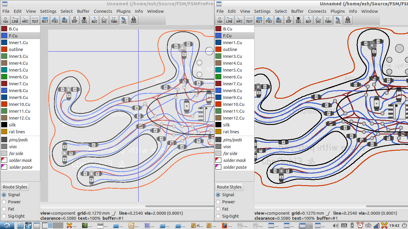
My usual PCB layout editor is pcb-rnd, a fork of the gEDA PCB layout tool.

The pcb-rnd project has been on a bit of an import/export module frenzy lately, and when FidoCadJ was stumbled upon, the natural thing to do was to implement an export module to FidoCadJ layout format.

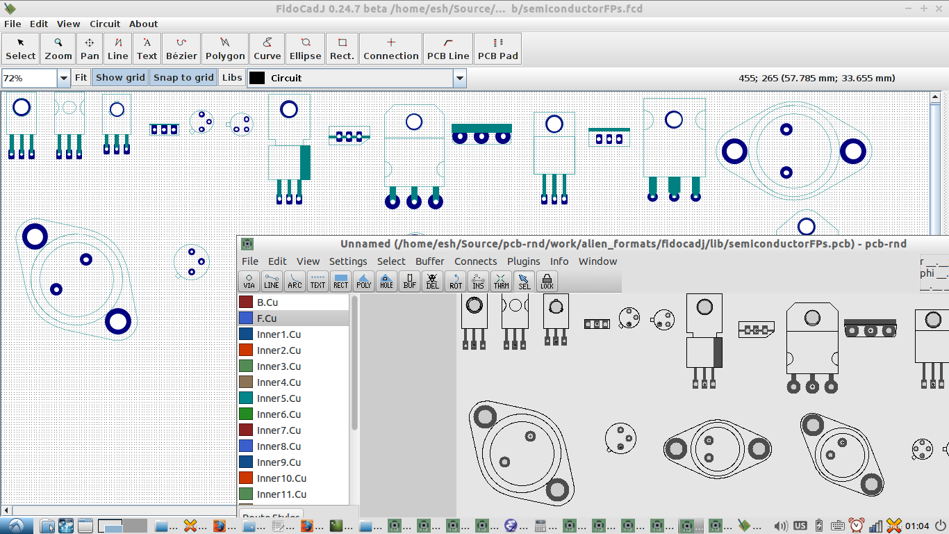
FidoCadJ is an easy to use cross platform Java application that allows schematic creation and also PCB board layout. It has a 5mil grid, and a good library of basic footprints. It is a successor to FidoCad, a C++ program first used in the 90s in Italy to share schematic and layouts on Usenet in a compact format.

FidoCadj exports in a variety of formats, including SVG, pdf, and ps, but lacks Gerber output. It does, however, natively support cubic beziers and cubic splines.

Excited by the possibility of a very natural and simple method of achieving freeform, artistic track and outline design on PCB layouts, the logical thing was to add an export module to FidoCadJ to export pcb-rnd/PCB (.pcb) layouts which would include the beziers and cubic splines converted to line elements.

The FidoCadJ repo was cloned locally, and emacs was fired up.

The FidoCadj code is very nicely structured, and I was able to use an unpopulated skeleton for an Eagle export module that was there as a basis for the gEDA exporter.

FidoCadJ is interesting as it expresses footprints and symbols as a one line "macro", which is defined in libraries. Default standard library macros are not routinely "exploded" on saving, but non-standard, local macros can be.

The FidoCadj exporter code allows macros to be dealt with by the exporter module, or "exploded" into primitives by the Export "overseer" code which can then be submitted individually for processing by the currently invoked exporter.

In the case of gEDA pcb-rnd/PCB, footprints primitives are not a subset of the layout elements, and have slightly different formatting. For this reason, the exporter code has to explicitly deal with the full macro definition and do its own parsing, returning footprint appropriate primitives wrapped in a single footprint Element[]() wrapper in the layout file.

Once this was appreciated, implementation of the exporter proceeded smoothly.

A motivated Java coder could implement a similar exporter for KiCad if keen, but pcb-rnd exports to Kicad anyway, and can be run headless as a command line batch conversion utility, so it would now be a bit of a duplication of effort for a KiCad user to code an exporter in FidoCadJ.

The FidoCadj exporter code has been cleaned up to suit the FidoCadJ style guide, and has now been incorporated into the FidoCadJ git project mainline.

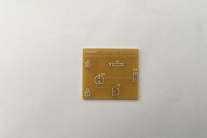
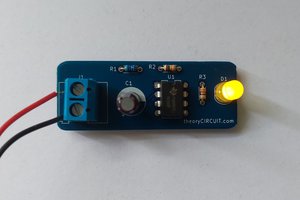
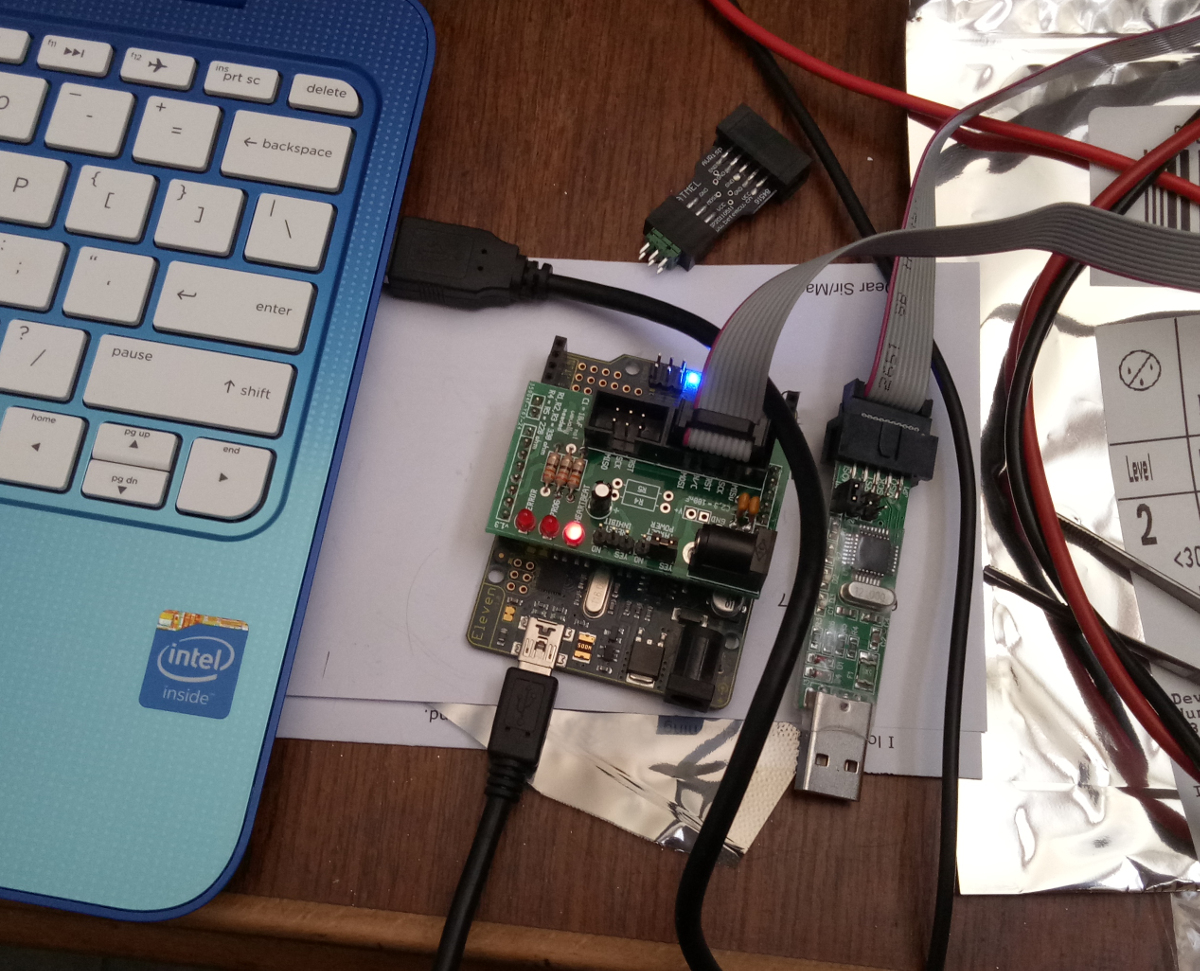
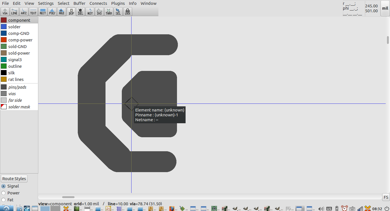
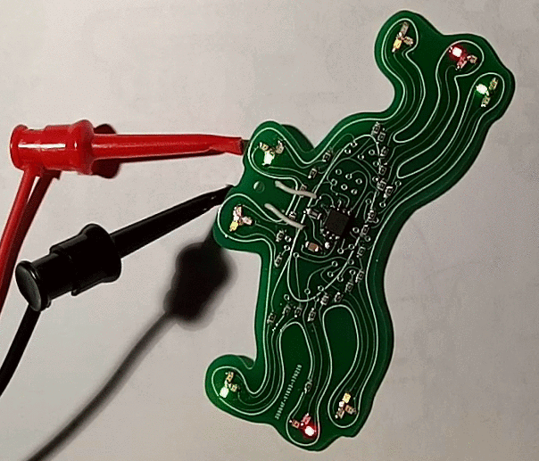
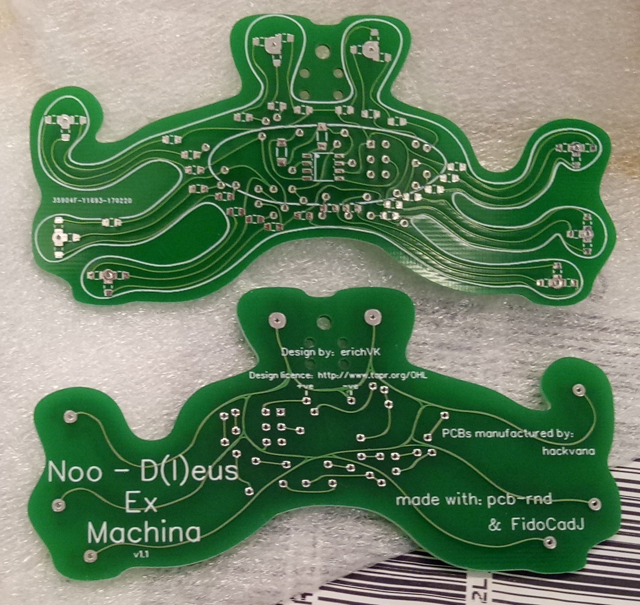
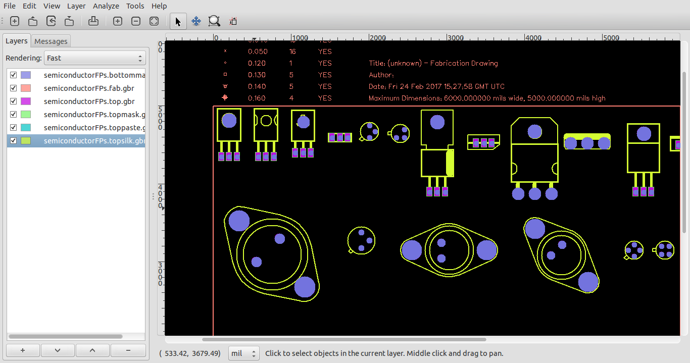
Import and export code like this requires testing, and to test the newly implemented, a suitable layout was conceived....

main.c

code using pins on current flying spaghetti monster PCB version for current LED bus configuration. One could use pin 7 as an ADC input for flashing speed via a pot, but this would shift the output function to pin 5. Code changes would be needed for this.

x-csrc - 1.26 kB - 03/11/2017 at 05:56

Download

blinky.hex

Attiny85 firmware to flash the three LED buses in turn, each one on for about 200ms, total duration of cycle is ~840ms.

hex - 672.00 bytes - 03/11/2017 at 03:38

Download

FSMPreProductionFinal-v1-0.pcb

Initial layout in gEDA pcb-rnd/PCB (.pcb) format. 50mm x 100mm board outline done in pcb-rnd to set constraints. The layout was then exported to FidoCadJ format. Freeform design of outline layer, silk screen and tracks on top and bottom copper done within FidoCadJ. At this point the design was exported back to gEDA pcb-rnd/PCB format for final touches and export to gerber for manufacture.

x-pcb-layout - 965.05 kB - 02/17/2017 at 15:18

Download

  • pcb-rnd... now with GL rendering...

    a103918103/11/2017 at 09:49 0 comments

    the current svn version of pcb-rnd now has GL support.... so as well as looking nicer, working on the ~ 1MB layout for the next version will be quicker!!

    GL rendering on the left, and vanilla gtk2 rendering on the right:

    Soooo fast,...

  • Programming the attiny85 with an Arduino uno as ISP

    a103918103/11/2017 at 06:17 0 comments

    In the picture you can see the cheap ebay USBASP clone being updated with the arduino uno acting as a programmer.

    You can also see the 10->6 pin adaptor being used as a "pogo pin"-esque "hold in place" programming fixture.

    In the end I used the Arduino as ISP to program the flying spaghetti monster PCB, and didn't use the USBASP at all.

    The important thing for success was having a programmer which could be used at 9600 baud by avrdude from the command line.

    As far as bringing the toolbox to build the plane before you get on it, the Arduino is sporting a shield I designed in gEDA PCB some time ago for this sort of use. So, even the tools were built before arriving at the airport to build the plane!!

  • Ideas for v2 of the flying spaghetti monster PCB

    a103918103/10/2017 at 22:06 0 comments

    I've made a solderable link footprint in pcb-rnd, and will add them to the revised layout for the three LED power distribution networks. This will simplify programming as well as testing after assembly.

    I think I'll add support for the solderable link footprint as a paremtrically defined element; it only needs a simple awk script and glue code.

    I might also add pads for a resistive divider so that the ADC on the spare pin can figure out what speed to flash at, so that one lot of code can be used for FSMs flashing at different rates, simply configured during construction with the right resistor network.

  • First Flying Spaghetti Monster PCB completed, attiny85 programmed

    a103918103/10/2017 at 13:04 0 comments

    After an evening of hand soldering, and careful checking with the multimeter to make sure the light emitting diodes were the right way round, the first FSM PCB was finished.

    I could not get the arduino IDE to behave with an attinty85 as the output target. After some hours trying different versions of the IDE, installing updated configuration files for avrdude, and support for additional models of attiny in the IDE, I concluded that baud rates over 9600 were doomed to fail.

    Testing with avrdude on the command line showed that the target was alive and indeed an attiny85, when probed with 9600baud.

    In the end I knocked up some c code, built is with avr-gcc, and then used avrdude to upload it at 9600 baud.

    I will put the code up when the dev machine is nearby. In the meantime, the design file needs a few tweaks to make assembly and testing easier. So... don;t run off to order those pcb's just yet.

    The main things to improve on the layout are

    1) make the ISP header holes a bit bigger, although they worked fine as a "hold in place" set of contacts for programming.

    2) add jumpers or solderable links so that the MCU can be programmed by the programmer without interference from the LED networks

    3) maybe make provision for a reverse polarity protection diode

    4) add a track that was missing between reset on the MCU and the ISP header

    5) add a track missing between pin 6 and its LED network, perhaps with a solderable jumper.

    6) make the MCU footprint pads a touch bigger, to make hand soldering easier

    Overall, I'm pretty happy with the pcb-rnd -> fidoCadJ -> pcb-rnd workflow...

  • Flying Spaghetti Monster components have landed

    a103918103/09/2017 at 06:35 0 comments

    Time to warm up the soldering iron for the flying spaghetti monster circuit boards...

  • The Noo-D(l)eus FSM PCBs arrived from hackvana

    a103918103/01/2017 at 21:49 0 comments

    It's a bit like the joke about Unix airlines; you bring the toolbox to the airstrip, build the plane exactly how you'd like it, then fly it wherever you want to go....

    The cubic splines, cubic Bezier tracks, footprints and other features made it into the pcb-rnd layout and thence to gerber thanks to custom export module code written for FidoCadJ... and the stroked font used on the PCBs is the Hershey Sans Stroke font, faithfully ported from EggBot font description files with custom code a while back...

    Next up... populating the boards...

  • FidoCadJ code git pull request done

    a103918102/26/2017 at 12:48 0 comments

    The export module code has been submitted to the FidoCadJ mainline from my fork

    https://github.com/erichVK5/FidoCadJ/

    Anyone wishing to give export to gEDA pcb-rnd/PCB a go before the new export module is integrated into mainline can build from my branch.

    you simply git clone the repo

    cd into it the directory, then

    "make rebuild"

    assuming you have the usual toolchains and Java installed

  • PCBs on their way

    a103918102/26/2017 at 12:43 0 comments

    DHL sent an SMS telling me that my hackvana PCBs are on their way... yay!!

    Not long now!!

  • Further refinements to export code

    a103918102/24/2017 at 15:43 0 comments

    The text is behaving pretty well with round trip testing pcb-rnd -> FidoCadJ -> pcb-rnd

    and footprints have been improved with circle, silk rectangle and minimum line thicknesses for silk elements

    If all goes well, there should be some FidoCadJ equivalent footprints on gedasymbols.org soon....

    And here's an example gerber output of the Semiconductor footprints....

  • Fine tuning of pcb-rnd export to FidoCadJ

    a103918102/23/2017 at 14:46 0 comments

    Did a bit of troubleshooting to improve the round trip with text on the PCB, when going from pcb-rnd->FidoCadJ->pcb-rnd. I think there might be a subtle scaling issue in FidoCadJ when loading text orientated at 180 degrees. I'll need to sniff around their loader/parser a bit... not that text is really expected to make the round trip losslessly, given differences in font rendering and formats. The end user would have to touch up text most times even if the scaling is behaving properly.

    I also managed to build pcb-rnd on an android phone within gnu-root. It really needs a mouse for use though. A good example of the portability of C code.

    I also got FidoCadJ's android app to work on the same phone.

    A keen hardware hacker with a phone or android tablet and a scroll mouse could theoretically design and export gerbers for manufacture, all on the portable device...

View all 14 project logs

Enjoy this project?

Share

Discussions

Similar Projects

Does this project spark your interest?

Become a member to follow this project and never miss any updates