 Bruce Land
-- Video input from NTSC to VGA
The board supports NTSC/PAL input through a Video Input subsystem
in Qsys. A camera is attached to the yellow composite video jack.
Several modifications need to be done to the Qsys layout and top-level
module to make this work at 640x480 resolution. In the Video Input
Subsystem:
- Video_in_rgb_resampler module changed to output 8-bit rgb
- Video_in_clipper module set to 8-bit, 1-plane
- Video_in_scaler module set to 640x480 with width scale 0.5, height scale 2.0, 8-bits, 1-plane
- Video_in_DMA module set to 640x480, 8-bits, 1-plane
In the top-level module the video input signals need to be defined as given in the reference design, but the TD_RESET_N signal is not correctly generated by the supplied IP, so a line was added to the top-level assign TD_RESET_N = SW[1];
. The switch may need to be cycled at power-up to enable the system.
Turning off the switch freezes the video capture. Also, the system would
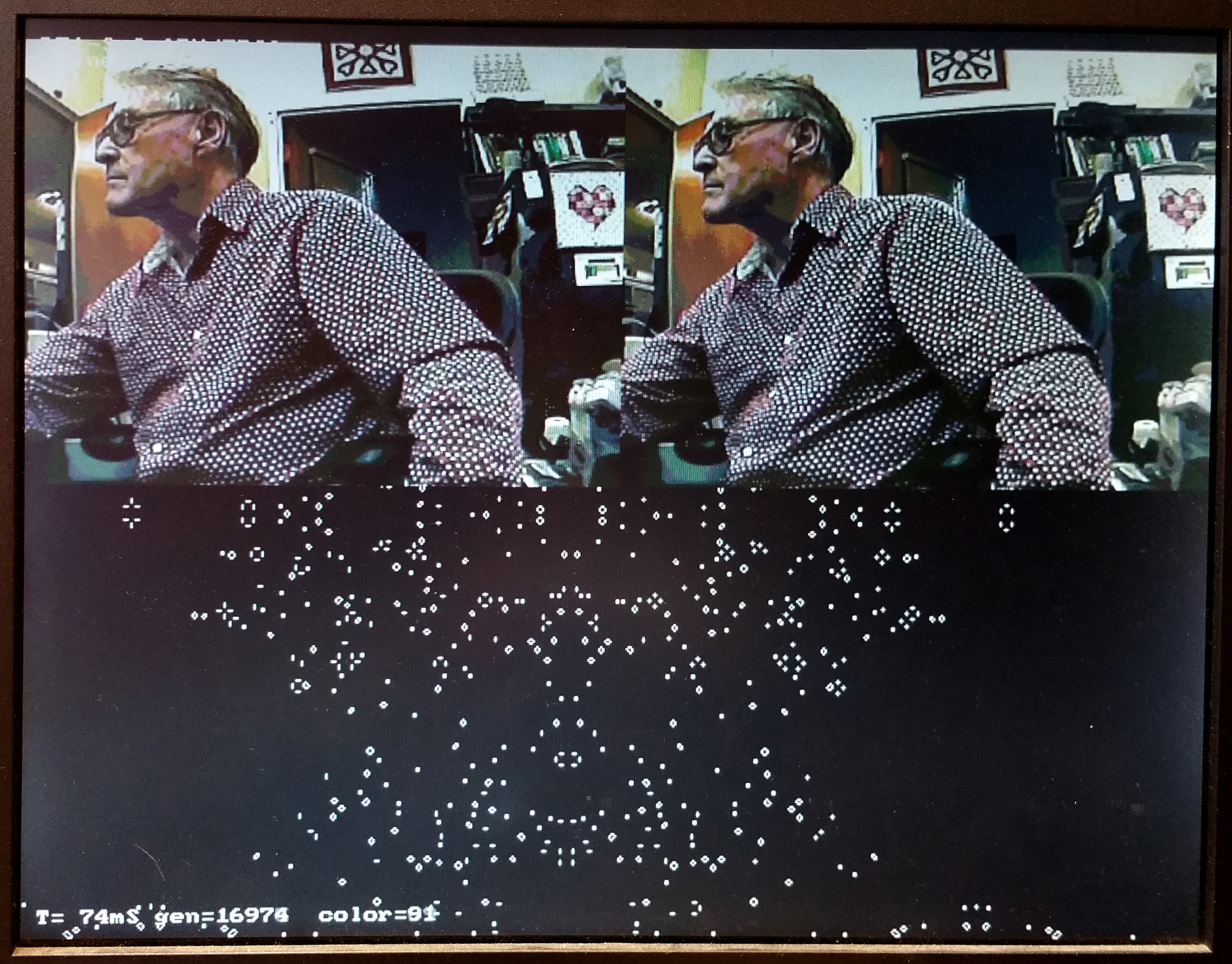
not start unless the edge-detect option was transiently turned on by a HPS program. The
HPS program also reads and displays the 8-bit color of the pixel at
video input location 160x120, the middle of the input image. I do not
know yet why there are two copies of the camera image displayed.
(top-level, project ZIP).
---- Video input from NTSC to on-chip-memory, then to VGA using HPS
The Qsys layout can be modified so that video input goes to
on-chip, dual-port SRAM, while the VGA display is refreshed from SDRAM.
It is then possible to use the HPS to copy pixels from the video-in SRAM
to the display buffer SDRAM, or just use the pixels for computation on
the HPS. Changes to the Qsys layout:
- The VGA subsystem
- Inside the VGA subsystem, the vga_pixel_dma module has the address modifed to 0x00000000, the base of SDRAM.
- Output from the dma controller in the top-level Qsys is disconnected from on-chip-sram
- The AXI-bus master remains connected to SDRAM so that the HPS can read/write VGA screen
- The Video_in subsystem
- Inside the Video_in subsystem, the video_in DMA controller is set to address 0x08000000, with size 320x240
This address corrresponds to the Qsys bus address of on-chip RAM. - Output from the dma controller is routed to port s1 of the on-chip-sram
- The AXI-bus master is connected to port s2 of the on-chip-sram
- Inside the Video_in subsystem, the video_in DMA controller is set to address 0x08000000, with size 320x240
 A
A
HPS program can read/write the video_in RAM and the VGA display SDRAM
to copy the pixels from video in to display. There are new functions to
support the read/write. As before, switch SW[1] must be UP for the video
input to run. Using the HPS (instead of an Avalon bus-master) is
inefficient use of the bus, but is useful for testing. A slight timing
error results a one pixel ripple in the video input diaplay. (HPS code, project ZIP).
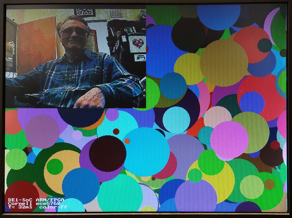
Down in the lower-left corner, the time readout gives the copy-time of
about 30 fps. The color indicator reads white, which is the one-pixel
dot on my neck, inserted by the program at (160,120) in the video-in
buffer.
There is a newer version which does the input copy to VGA completely in hardware. See http://people.ece.cornell.edu/land/courses/ece5760/DE1_SOC/HPS_peripherials/Bus_master_slave_index.html about 2/3 of the way down the page
 Matty
Matty
 jasoneppink
 Leon
Leon
 Keith
Keith