 helge
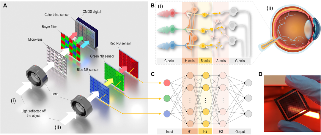
helgeA news flash on Hackaday (1) highlights recent work (2) on using Perovskite pixel mosaics to implement multispectral imaging. Similar to Sigma Foveon sensors, layers can be stacked in the optical path to obtain a spectral decomposition of the incident light rays.
The reconstruction is achieved through fitting of a set of coefficients which approximatively encode the inverse transform to the spectral cross-talk owed to overlapping absorbance spectra and incomplete extinction (= "neuromorphic" in fancy-speak).
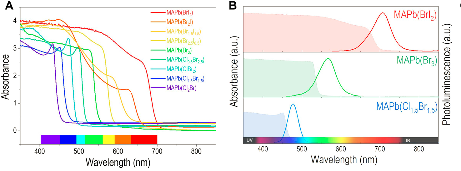
Depending on the chemical composition, different absorption edges are found:
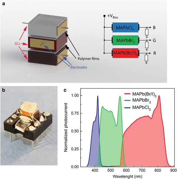
Unlike the Foveon sensor though, at this stage, the authors do stack this sensor together with individually spin-coated, laser machined and pre-qualified single-Perovskite sensor planes:
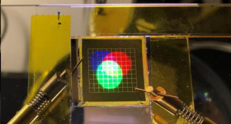
"Figure S28 displays the testing setup, where we used a projector (M6 Pico Projector, AAXA Technologies) to generate a panchromatic source image and used a lens to focus the incident light onto the chips. Blue, green, and red chips are sequentially stacked (six-terminal stacking) from front to back, where blue, green, and red channels of current are read out independently."
Which is fine for the paper, but points at the compounding difficulty of 2.5D integration - a factor which translates into years of research and a super-linearly growing difficulty in adding more and more spectral bands.
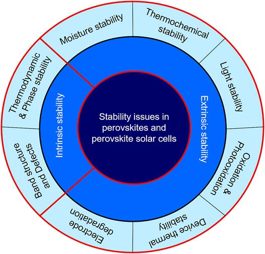
Perovskites are envisioned to be put on plastic foils (3) for solar photovoltaics applications, but here sensors can be kept under vacuum or inert gas in hermetically sealed ceramic packages with glass windows, eliminating some of the stability issues with this class of materials (4):
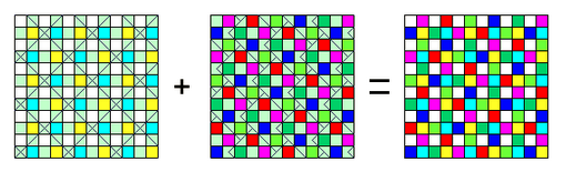
But if I were to bet, I think it's more likely we'll see Bayer pattern and, at best, 4-6 wavelength sensors with more elaborate CFA-like patterns (5) before high integration happens:
 For the proclaimed satellite imaging applications (if lifetime issues can be controlled), sequential stripes in push broom imagers should rule out the need for intricate, low-yield stacked pixels.
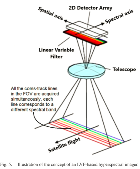
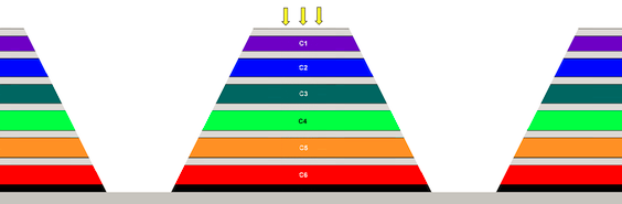
Addendum: just how hard can it be? "Non-dissipative internal optical filtering with solution-grown perovskite single crystals for full-colour imaging" (7) has you covered:
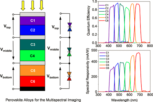
(Note: the C1-C2, C3-C4 and C5-C6 stacked perovskite layers should be similar to gradient engineered light absorption layers, not anti-series diodes. The illustration is a bit strange in that regard. Figures S14 and S15 show adequately contacted organic diode structures as well.)
"Direct contact of perovskite layers appears challenging in the view of known halide-ion mixing. This problem might be mitigated by insertion electrically conductive, optical transparent and halide-ion-impermeable contact layers."
Essentially, some form of mesa etching, passivation, barrier contact formation and metalization would need to take place, as sketched below:
 This looks a lot more involved than the initially advertised simple spin coating process and resemble what is being done to form III-V diode structures (9) and lasers.
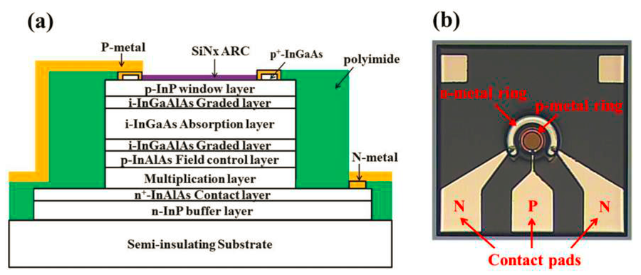
References
- https://hackaday.com/2023/06/02/perovskite-sensor-array-emulates-human-retina-for-panchromatic-imaging/
- https://www.science.org/doi/10.1126/sciadv.ade2338
- https://onlinelibrary.wiley.com/doi/full/10.1002/adem.201901217
- https://www.frontiersin.org/articles/10.3389/felec.2021.712785/full
- http://www.quadibloc.com/other/cfaint.htm
- https://doi.org/10.1109/JSTARS.2021.3090256
- https://www.nature.com/articles/am2017163
- https://pubs.acs.org/doi/10.1021/acsami.1c25095
- https://doi.org/10.3390/s19153399
Discussions
Become a Hackaday.io Member
Create an account to leave a comment. Already have an account? Log In.