 Jon Buford
The first 3D model of the RPi HAT module helped to solidify the overall design approach.
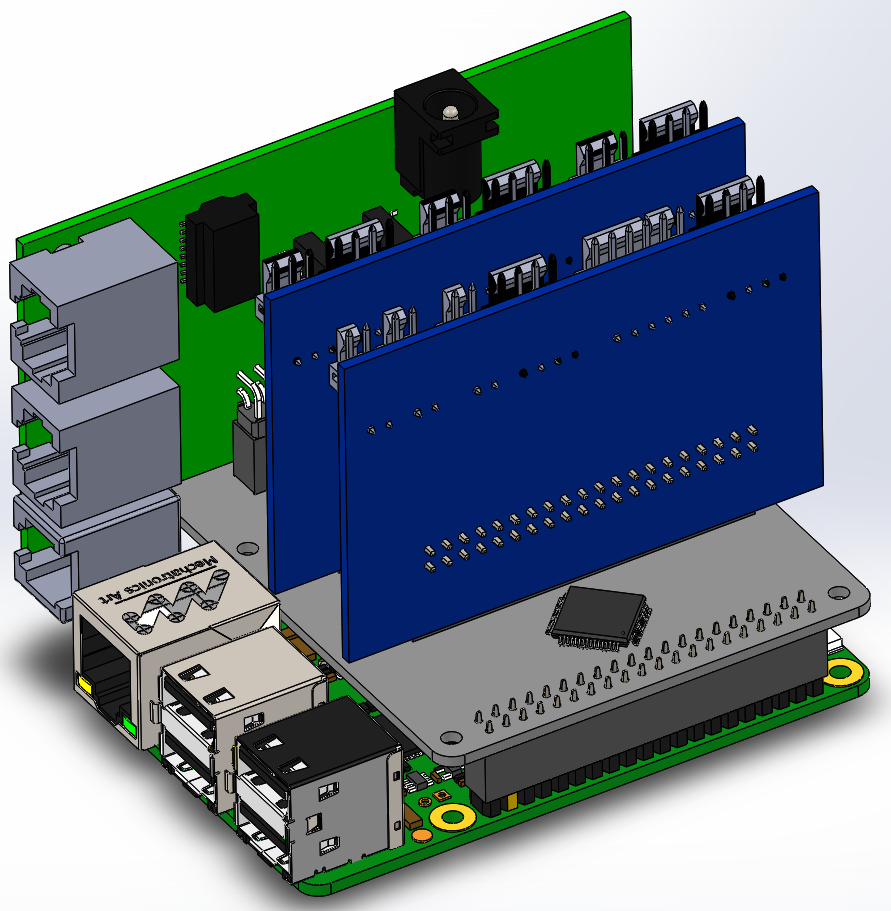
What you can see here are two standard powered (40-pin) IO modules and in the back is a POE Power module. This is a good configuration to design around because the POE module extends down below the plane of the Connector module and has the network jacks at the same face as the Raspberry Pi. So, going with this constraint, I've placed the Power module at a reasonable distance from the Pi connectors and set that position. Another option would have been to place the power on the other side, above the HAT connector. That would have resulted in the POE connectors on the other side than the Pi connectors and it also makes the power routing not possible with a standard HAT board footprint.
On the other hand, this layout is close to the existing Connector modules, so the layout work done for those will be a good reference.
I've placed the two modules at a spacing of 0.7 inches (2.54mm*7) to allow for standard proto board to be used to build a combined 2 IO module board, and the power is at 0.8 inches (2.54mm*8) for that same reason. This results in the layout shown (when combined with the constraint of keeping the power connectors clear of the Pi connectors).
Now, that fully constrains the interfaces of our design, and gives us a PCB with placement of all connectors. The next step is to then look at what MCU to embed in the design. Shown in the 3D model is a 64-pin LQFP, which is about the largest component we could practically put in. But, we need to consider cost and functionality to make some tough design decisions.
The biggest constraints to consider are wanting a more robust MCU for both helping to isolate the Pi but to also make this a good starter board for people with Atomo. Given my current experience with NXP Kinetis line ARM based MCUs, the only option there is the KE line. Of those parts, the KE02 line is the least expensive, with parts available in the $1 USD range. The KE04 line is similar, but it has been designed to complement the KE02 line so it has a smaller part and then larger parts, but the KE02 line for 44-pin components is a pretty sweet spot for the number of pins and all other requirements. The 40MHz version starts with just 16KB of flash and 2KB of RAM, but that should be OK for very basic applications or setting this up as an IO expander for the Pi.
Moving up to a 64-pin package also comes with more memory, so the step up is about $0.40 USD. Since the other constraint for the design is to try to fit it into a $2.50 BOM cost, that $0.40 is going to come at either a cost of increasing the retail price or sacrificing something else, if there is anything else to sacrifice. Assuming the basic costs are:
| ITEM | QTY | Cost | Total |
| PCB | 1 | 0.7 | 0.7 |
| MCU | 1 | 1.08 | 1.08 |
| Connectors | 4 | 0.15 | 0.60 |
| Misc | 1 | 0.2 | 0.20 |
| Total | $2.58 |
We can probably just get the design into our target with a 44-pin component. Otherwise, we will need to step up the retail price.
So, the next question is what can you functionally do with that 44-pin part? That will be the next log entry.
Discussions
Become a Hackaday.io Member
Create an account to leave a comment. Already have an account? Log In.