 Nick Sayer
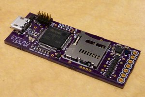
Orthrus dramatically simplifies the problems of providing a securely encrypted data store. There are no passwords or key material to manage. The act of pairing two cards together automatically creates all of the key material necessary to secure the store without any human action (other than initiating the paring process by pressing and holding a single button). The security offered by Orthrus is simple to explain and trivial to use. It's simply that if you have both of the cards, you have the data. If you have only one of them, then it is cryptographically opaque.
The first block of each card is reserved as a key storage block. The size of the volume reported to the USB host is determined by taking the smaller of the two card sizes, subtracting one and doubling that. The first block on each card contains a structure with the following:
- A magic constant compiled into the firmware to identify the card as belonging to an Orthrus volume.
- A flag bit identifying the card as either the "A" or "B" card (the cards can be inserted in either order and it should still work).
- A 64 byte volume ID.
- A 32 byte card key value.
- A 16 byte nonce value for the block tweaking (of which 12 bytes are used).
When the device is initialized (either when its inserted into a host with two cards already installed or when the second card is inserted), each of the key blocks is checked. If the magic value is wrong, or if the two volume ID values don't match or if there isn't one "A" and one "B" card, then the error light is turned on and the volume isn't mounted. This prevents cards inserted mistakenly from being corrupted. To bootstrap, there's a button on the board. If the button is pushed while the error light is on, then the two key blocks are initialized and the device made ready.
If the pre-initialization checks succeed, then the two card key values are shuffled together (in "A" "B" order) to make a 64 byte buffer. The two halves of this shuffled data is fed through AES CMAC with an all-zero key, with the two results concatenated together. The result of that becomes the new AES key and the CMAC is run over the two halves of the volume ID, again, with the two results concatenated together. The result of that becomes the AES key for the volume. At that point, the drive is ready.
To read and write individual blocks, AES XEX mode is used. The incoming block number in the request is translated by using the LSB to select either the "A" or "B" card. The rest of the block number is right-shifted once and 1 is added to make the physical block number for the card. The XEX mode uses a 16 byte nonce. The nonce consists of the first 12 bytes of the nonce value stored on the opposite card from the one being read or written, concatenated with the (logical) block number. The nonce is encrypted with the volume key to form the first "tweak" block. For each 16 byte AES block of the disk sector, the plaintext is XORed with the tweak block, then encrypted with AES ECB mode, then XORed again with the tweak block to form the ciphertext. Decryption is the same, except that an AES ECB decryption operation is performed in the middle (the tweak is still formed with an ECB encryption). After each block is processed, the tweak block is transformed into a new tweak block by multiplying it by 2 within a Galois Field of 2^128 (I confess I don't really understand GF math properly - I just read a bunch of examples and pseudocode on the net) and then is ready for the next 16 byte block.
In an earlier iteration of Orthrus, AES counter mode was used, which allowed us to precompute the cipher stream bytes for XORing with the card data, but counter mode has some cryptographic weaknesses that make up for the speed advantage that background precomputation affords. XEX mode can't be precomputed, and unfortunately gives us a 33% speed penalty, but is the mode used almost universally for whole-disk encryption (most implementations actually use XTS, but if the sector size is divisible by the encryption...
Read more »


 Blecky
 J.C. Nelson
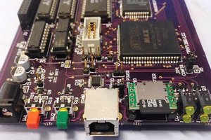
 tomcircuit
 Jonathan 'theJPster' Pallant
Took a look at the new version of the schematic, overall it looks great. Some obvious big improvements (simplifications, really) compared to the previous AVR-based design. Getting rid of all that hardware RNG is a big win. This new design definitely seems much more by-the-book, which is rarely a bad thing. Some more specific comments:
- Looks like the LEDs, buttons, high-side card power switch, SD card slots, and 3.3V buck are all holdovers from Rev 2. So all that stuff should be proven already, nice.
- USB looks mostly the same, but with the ESD consolidated. Checked that, looks good.
- The bus-mux looks good. Takes a minute to understand IC2 and IC3 are essentially one "thing" doing one job but it's simple once you understand. It looks like the mux chips may be both missing their bypass caps?
- Right now you've got a single signal "/CRDEN" applying power to the SD cards *and* enabling the output drivers on your data mux. That's clever and likely fine, but considering you have crazy IO left over, consider separating those into two control signals. CRDEN_PWR and CRDEN_DATA or something. There may turn out to be some benefit to being able to sequence those slightly (power first, wait a beat, then data?) and even if there is no benefit, this change costs nothing in dollars or performance. Put them on the same logical port for the ARM and they can switch simultaneously.
- I would also consider adding a discrete pullup (1kΩ - 10kΩ) to the CRDEN signal(s) to guarantee that those parts stay hella off (esp during power-on) until the ARM explicitly turns them on.
- Considering the short distances covered by these traces, and the likely good slewrate control (etc) offered by the ARM, I doubt signal integrity vis-a-vis rise times, reflections is going to be an issue at all. BUT if you haven't done at least a very basic estimate of this it's probably good to do it, just to prove to yourself. It may turn out to be smart to add source termination resistors to the ARM, the mux, or both.
- I said no nits, but here's a little one anyway. R12-R14 are the only discrete 100kΩ resistors in the design. If the array part you use for R19 is cheap, consider using it again instead of those discretes. Might be worth it to drop a line from your BOM and get rid of a couple placements. If you can add the CRDEN pull-ups (recommended above) to the second array, it'd be almost half full. Not bad.