 Marcel van Kervinck
The joy of using hypermodern multiple e-beam direct-write lithography to "advertise" TTL technology from the 1960s... This is an electron microscope image of the Gigatron startup screen. This time it isn't displayed on a VGA monitor (or on a supercon badge), but printed on a silicon test wafer as used for IC making. The image was printed using a Mapper FLX-1200 e-beam writer. For comparison, a human hair is typically 75 µm in thickness.
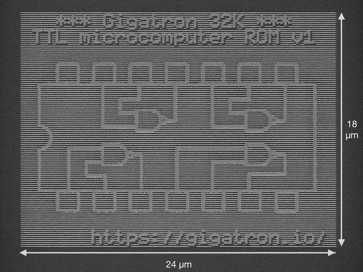
The Mapper principle is much like that of an ink jet printer head with hundreds of nozzles, except we're using accelerated electrons here instead of ink, and silicon wafers instead of paper (and there are no colors). The beams each have a spot size of under 30 nm and they're scanning the surface with a positioning accuracy of below 3 nm. They're all perfectly stitched together to seamlessly cover the large area needed to make complex devices. The wafer was coated with a thin layer of resist material, and everywhere a sufficient number of electrons landed, an image formed that could be developed.
This tiny area of 24 µm x 18 µm shown above was printed in just a few milliseconds by a couple of hundred parallel and independently controlled electron beams, all focussed on the wafer in a high-vacuum chamber. This image is a small part of a much larger test pattern. The resolution is in the 40-50 nm range here. The e-beam writer has tens of thousands of beams all working in parallel. The data stream to support that is about 3 Tbit/second and is generated by a large rack filled with FPGAs.
A SEM is needed to view the result because the details are too small for optical microscopes. This super fast e-beam technology is developed to make new types of security ICs possible, but it has other applications in nano-fabrication as well (one is entertaining the engineers working with it).
The image contains a schematic of the iconic 7400 quad NAND chip, introduced in the late 1960s. An actual NAND gate, or even a single transistor from the day, would be much larger than this entire image. The typical line widths in those early days of IC manufacturing were in the order 10 µm.
Courtesy Mapper Lithography and CEA Leti.
[Edit 2019-02-11: Unfortunately, Mapper is no more. Looking for a job now! ]
Discussions
Become a Hackaday.io Member
Create an account to leave a comment. Already have an account? Log In.
Smaller than a single transistor in a 7400! That's hilarious.
Are you sure? yes | no
They have a lot of fun toys at CEA/LETI :-D
Are you sure? yes | no