0%
0%
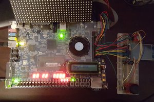
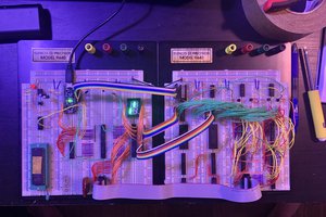
TMS9900 compatible CPU core in VHDL
Retro challenge 2017/04 project to create a TMS9900 compatible CPU core. Again in a month... Failure could be an option...
 Erik Piehl
Become a Hackaday.io member
Already have an account? Log in.
Just one more thing
To make the experience fit your profile, pick a username and tell us what interests you.
Pick an awesome username
hackaday.io/
Your profile's URL: hackaday.io/username. Max 25 alphanumeric characters.
Pick a few interests
Projects that share your interests
People that share your interests

 Matt Stock
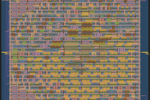
 Tim
Tim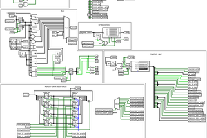
 Tim Ryan
This project has the potential for all of us TI 99/4A types. I am not technically anywhere near your league, but find this project very interesting. I saw your posts in Atari Age. I'm x24b over there, and here. Let me introduce myself, I'm Robert Webb.
The potential for a follow on machine to the 4A using this base is important, if that is a goal in the back of your mind. The now funded Kickstarter "ZX Spectrum NEXT" is a fascinating project breathing life back into a 30 year old product line. Maybe we have our own version, right here.
Thanks for your interest and motivation in one of my favorite machines. If nothing else, I'll follow your work here and smile every time I check in.
Best of Luck.