 Yann Guidon / YGDES
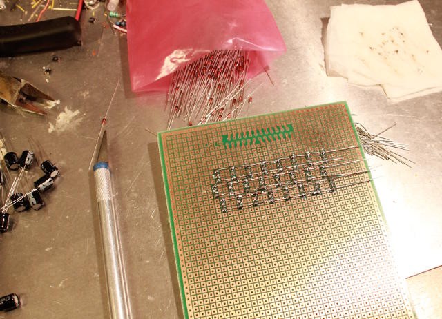
Following the recent updates about the DRAM (in the log DRAM (again)), I had to test all my assertions and try with the real parts.
The BAS70 are apparently not practical for a prototype because I have no suitable PCB. I'd have to put a lot of wires... But I found a method with the legs of two 1N4148 !
It was a pretty crazy adventure but it ends well (so far, if you don't count the 30 capacitors I soldered in reverse).
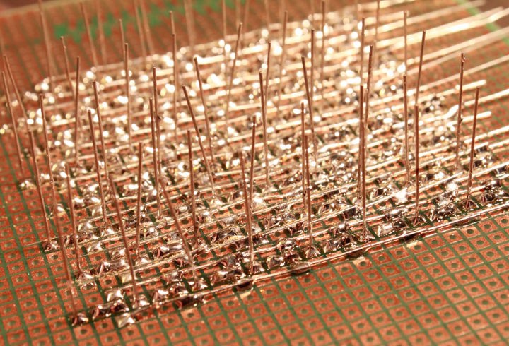
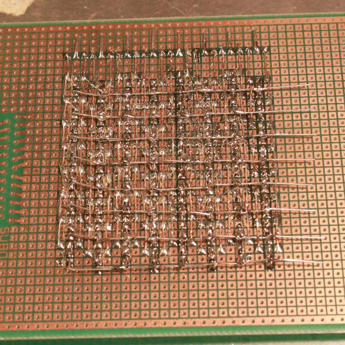
I figured out a placement that is feasible and compact, but it requires two levels of wiring. First, the diodes are soldered in place and their wires occupy the PCB surface :
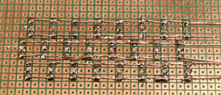
Make sure they are ALL in the correct direction :-) before it's too late...
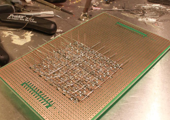
I have chosen to alternate the positions to prevent soldering problems :
of course, it's still important to test ;-)
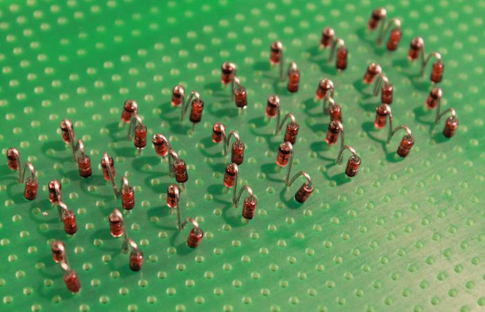
Then the capacitors. Make sure they are properly oriented ! (I wasted 30 of them...)
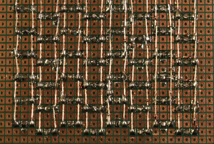
The positive side is connected to the diodes with a solder bridge and the other stands alone, waiting to be bent.
.
Side view :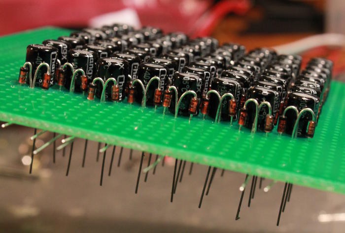
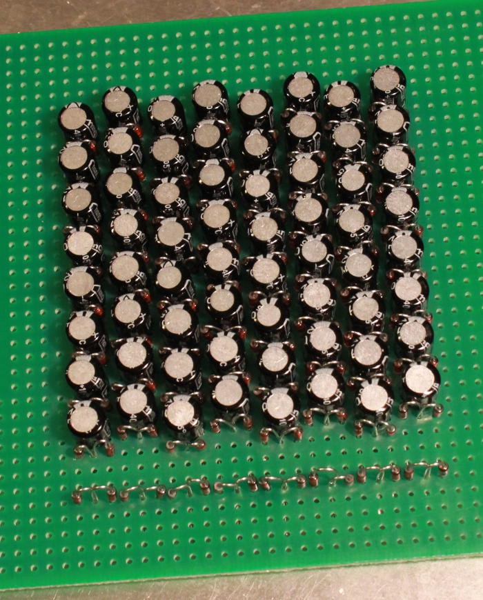
The finished board :
Tomorrow I'll wire some switches...
Discussions
Become a Hackaday.io Member
Create an account to leave a comment. Already have an account? Log In.
yann, are you still planning to connect this according to your earlier drawing https://hackaday.io/project/18757-ygrec16-ygs-16bits-relay-electric-computer/log/56214-new-dram-array ?
For accessing a row, you will need separate relay contacts for charge and discharge, as in the original Rory Mangles design. In your earlier drawing, each capacitor has 2 diodes, but for each charge diode, there is a current path in the other direction (through the discharge diode, then to the left side, through the two series diodes reaching the charge line. So each charge/discharge diode is shorted in the other direction through three diodes in series. Unless your working voltage is lower than 3 diode voltage drops (seems unlikely), this will not work.
Are you sure? yes | no
Hi,
yes i'm still using this approach because it allows one column to be accessed with several rows simultaneously, which brings *significant* savings in relays...
And I have chosen a high voltage system (24V as indicated on the drawing) to increase the stored charge, hence the retention duration and the tripping of the sense coils. The two diodes in series in the current path (I don't see how you find 3?) should not have a significant influence.
Of course... It's not yet tested.
Can you clarify your concerns ? Make a drawing ?
Are you sure? yes | no
I made a drawing for you:
The "red" diode is supposed to be "non conducting". But will that work, if the current can follow the green path to the other end of the "red" diode ? The same story goes for all other diodes connected to a capacitor.
Are you sure? yes | no
For current to pass, there must be a potential difference.
Only one column is connected to 0V at a time, so this limits the will of the electrons to flow somewhere else.
There will certainly be leakages but I can't know them yet, until I measure them...
Are you sure? yes | no
The diode is there to block one direction of current, isn't it ? But since the current can pass through the green path, the diode is not effective, and the circuit is essentially the same as if all diodes were replaced by shorts. In that case, all capacitors are "piecewise" connected to each other, as shown before:
I hope this can convice you ?
Are you sure? yes | no
I think I start to see what you mean... I'll have to investigate.
Are you sure? yes | no
That's the kind of problem where using SPICE would be usefull... Can anybody setup a sim ? I have no idea how to use that :-/
Are you sure? yes | no
I updated the log that you mentioned. Enjoy the illustrations :-)
Are you sure? yes | no
How many relays will your DRAM use?
Are you sure? yes | no
Basicly the relays are for MUXes and sending the pulses and data.
1 relay to write 0V or 24V to the line
1 relay to connect the column to the 0V
L-1 relays for MUXing the L×lines
C-1 relays for MUXing the C×columns
If L=C, then total cost is 2(L+1)
For L=C=16, that's 32 realays for 256 Bits (but 512 diodes !)
______
In practice, I have to test a theory with the prototype : we can drive several lines at once.
This way, the column MUX can be shared with all the bitplane, driving the relative bitcost down to maybe 18 relays/bit.
If the column drivers can be shared then I can reduce the number of line MUXs, down to maybe 8 and save even more. The column MUX would grow from 32 to 64.
cost: 63+(18×7)=190 only :-)
But leakage could become a problem. I must check before assembling so many parts !
Are you sure? yes | no
There might be an alternate to the wiring madness. I made a diode array in SIP - similar to those resistor networks for pull ups/down to a common rail. What I have is a strip of FR4 copper clad as the common on which one end of the diodes are soldered to while leave the other end open.
You can populate the opposite side of the FR4 for the other bus too i.e. make a dual row version. :) Pretty useful for protection networks for homebrew circuits as it reduces the crossing of tracks on your main PCB while actually improving on the performance - lower inductance.
Are you sure? yes | no
this is more suitable for a dense ROM array :-)
In the definitive DRAM, both diodes will be packed in a single SOT23 part.
For now, I will soon be ready to estimate the necessary refresh rate.
Are you sure? yes | no
Routing those would still be a pain as you have 2 busses that are running across signals at 90 degrees basically needs 2 layers. The SIP idea basically gets you another couple of routing layers for the rails.
Are you sure? yes | no
I'll use 2-sided PCB :-)
hopefully the 16×16 modules won't be too large, and they'll be easy to solder. 256 SOT23 then 256 capacitors...
What bothers me most is how to test them.
Are you sure? yes | no
I might order some relays and make one myself! I think it would help me understand your design so I can make DRAM with TTL better.
Are you sure? yes | no
forget about DRAM, just use thousands of 74HC574 :-D
Are you sure? yes | no
or an intel 2114 XD, Nah, Caps diods and relays are a bit special. I actually might use DRAM for the Registers on my #SBP-CPU (Slice Based Processor) project because I cant find the logic chips I need. It might actually work! Btw, excited to see how this works.
Are you sure? yes | no
(grabbing popcorn)
Are you sure? yes | no
*ahem* ferrite cores?
Are you sure? yes | no
(climbing in my hammock)
Are you sure? yes | no