 Yann Guidon / YGDES
work in progress, see also The instruction register (cont'd)
.
I've been focused on the main datapath but the control logic needs some love...
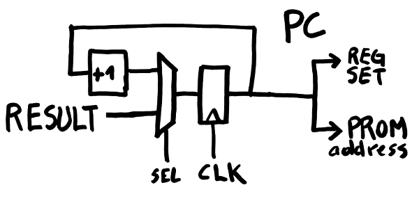
So let's talk about the PC, or Program Counter register.
From the user's point of view, PC is a user accessible register, that can be read as operand (only as the SRCX operand) and written as a destination. The value is incremented at every cycle to point to the next instruction so the value is visible both to the datapath and the PROM circuit.
From the hardware point of view : the PC is a register with a MUX2 (to select data coming from the datapath's result bus) and an incrementer.
How to use it and why
- Write an instruction address to PC so the next executed instruction is at the new address, as an equivalent of "BRANCH" or "JUMP" (it can be conditional)
- Read PC to perform operation on the current address and JUMP to a relative address
- Read PC to save it somewhere, just before you jump to a subroutine, to perform a CALL.
The last part requires a few MUX so the PC (actually, that's PC+1 so it returns to the next instruction) can be saved while the new address is computed.
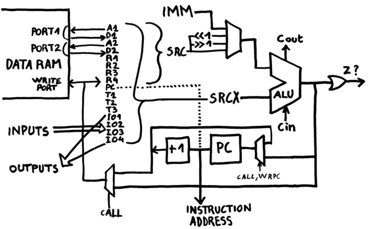
To select the CALL path, we need a bit or signal in the topmost bits of the instruction (to save the other buts and keep the whole architecture orthogonal). That's hard because all the combinations and fields have been used. Except one !
The "NEVER" condition is now renamed "CALL" and behaves as "ALWAYS" but enables the necessary MUX.
Concerning the width : since the PC interacts with the datapath (more than I had considered initially) it becomes part of the bitplane. So 16+2 bitslices will be implemented. The backplane will enable and route the proper circuits.
In practice, not all bits might be used. The PROM can reasonably (at most ?) contain 1K instructions (that's up to 24K diodes guys !) and the address decoder really gets large at this point...
The PC's MSB (topmost bits) could be used to store a few bits at your own risks, because I'd love to create a SRAM-based PROM emulator (controlled by a Pi, serving YGWM, yada, yada...) and I can easily use the whole 64K addressing space :-)
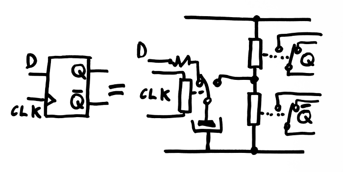
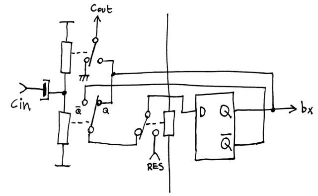
The PC's bits are implemented in CCPBRL, with a complementary output. Here is the equivalent circuit for a DFF : 3 relays and a capacitor are required, an additional resistor (in the 10-50 Ohms range) is added to reduce inrush current (and also protect from fast changing data if the input needs time to settle).
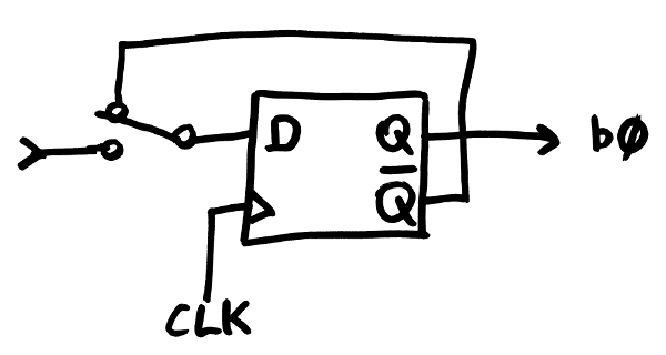
The LSB (or bit#0) is pretty simple : at each clock cycle, it toggles. So the inverted output is looped back to the input (through the MUX). Simple !
(actually, that's a simplification because the carry in will always be set to 1 and every bitplane will use the same circuit)
For the other bits, it's barely more complicated : a MUX2 selects between Q and /Q, depending on the "carry in" signal". The real trick however is to get this carry signal...
I know the usual method : the carry chain gets interrupted by a switch if the current stage is "1". That's method a) below :
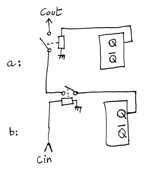
But this amounts to a AND gate, right ?
And a AND gate can have its inputs swapped, right ? So look at version b) for which the signal passes through the coil.
The great thing about this is that the fanout is 2, which is naturally implemented with a CCPBRL cell. A (hypothetical) single incrementer stage is shown below:
OK it slows the signal down... However, it's possible to
- alternate between circuit a) and circuit b) to halve the propagation delay
- include the carry chain switch's coil inside the DFF circuitry, but that requires 6V power and corresponding signals, to swing between 6V and 12V, and a resistor will waste energy
The incrementer should be quite fast because we want PC+1 at the same time the ALU delivers its result (so it can be written to the register and/or the memory).
The typical carry interrupted AND chain has a big problem with variable load (driving 16 relays can draw a lot of energy and damage the relays' contacts. But the PC+1 should be available in about 5 coil units (time to decode the instruction address, read/decode/amplifiy the control signals ...)
Discussions
Become a Hackaday.io Member
Create an account to leave a comment. Already have an account? Log In.