Patrick Van Oosterwijck
-
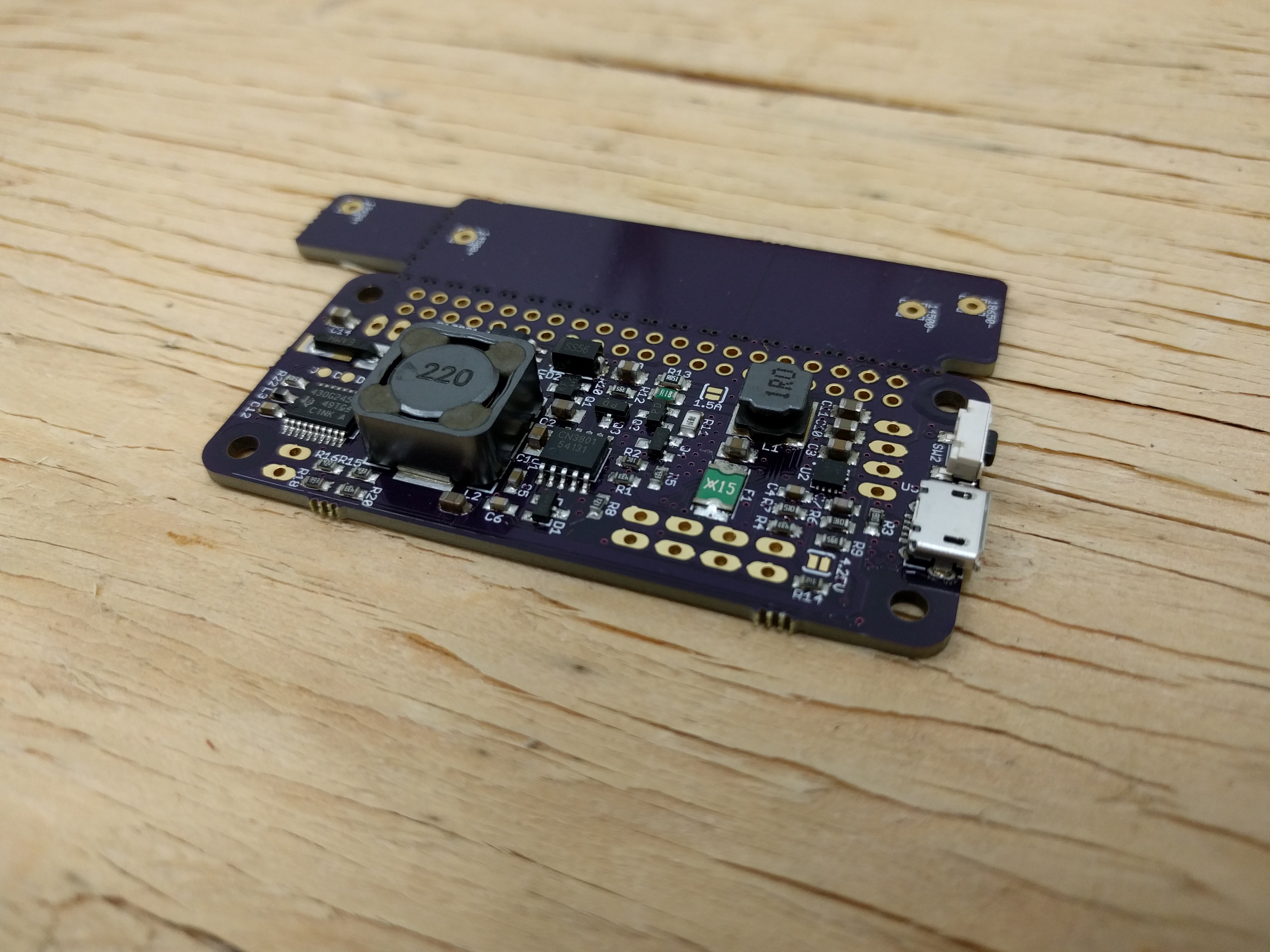
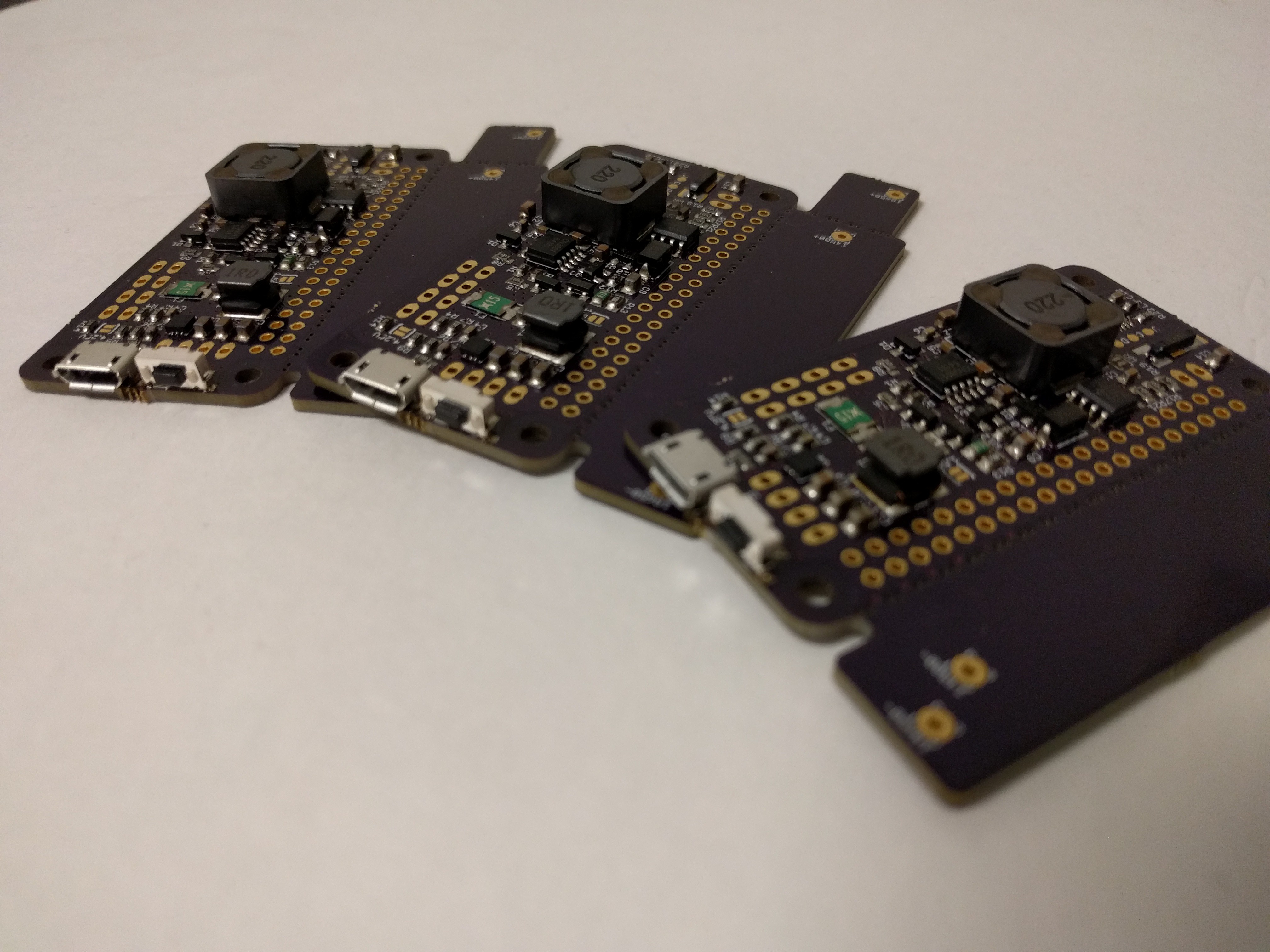
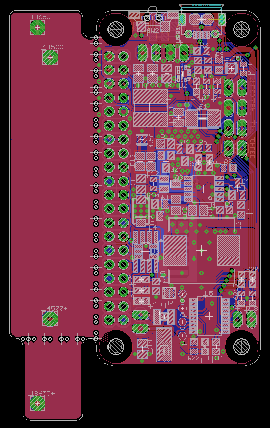
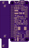
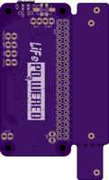
New prototype PCB layout
11/23/2017 at 18:59 • 0 commentsSince blowing out parts on my existing prototypes has gotten them to the limit of their useful life, it was time to get some new prototypes. :)
Time to make some changes related to things I've learned:
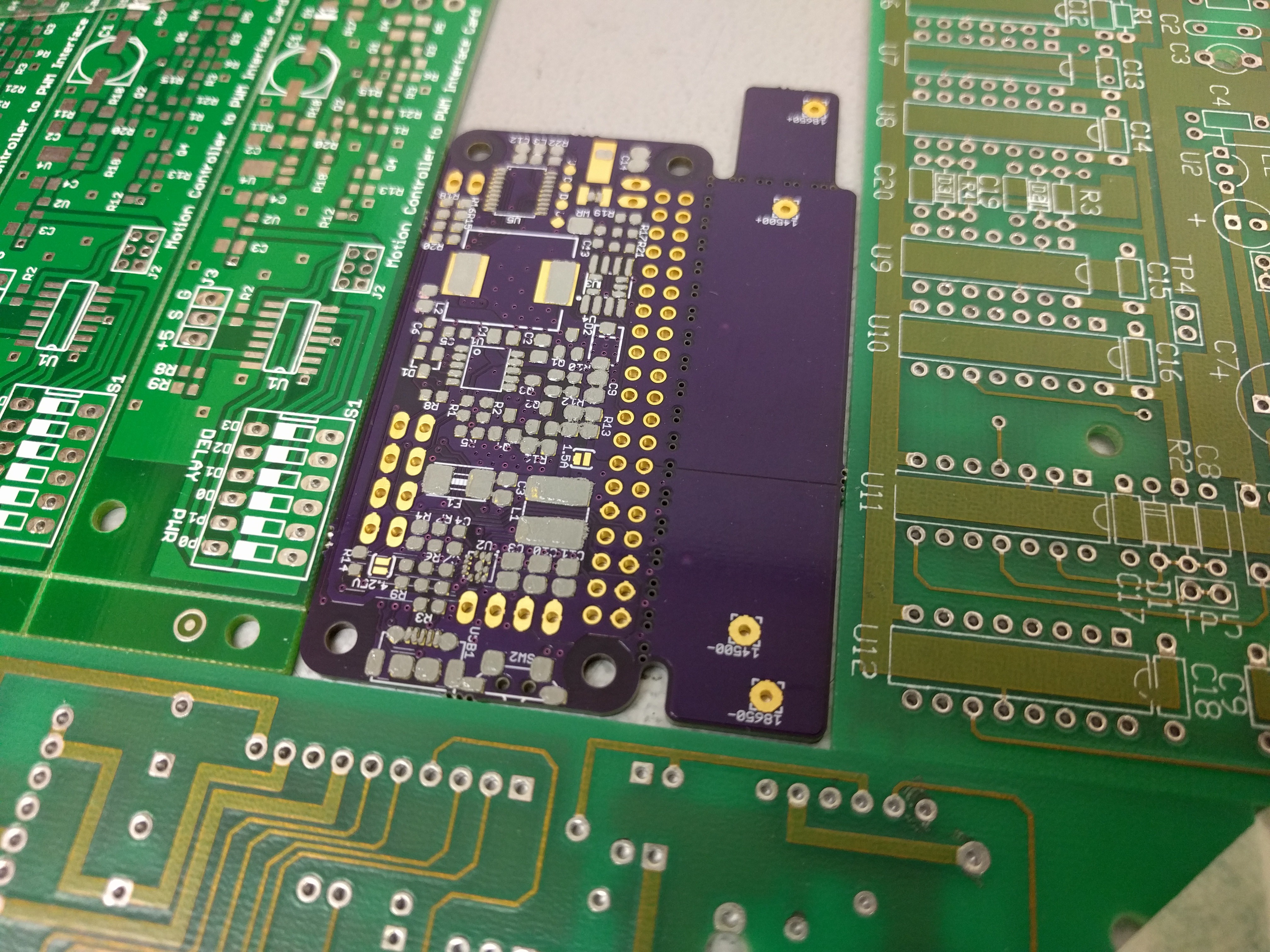
- The locations of the mounting holes for the 14500 battery was wrong on the first prototype layout so I fixed that. I also added extra holes to be able to mount the battery with a little gap so it's possible to mount the Pi in a case and have the battery outside. This should work with the official case.
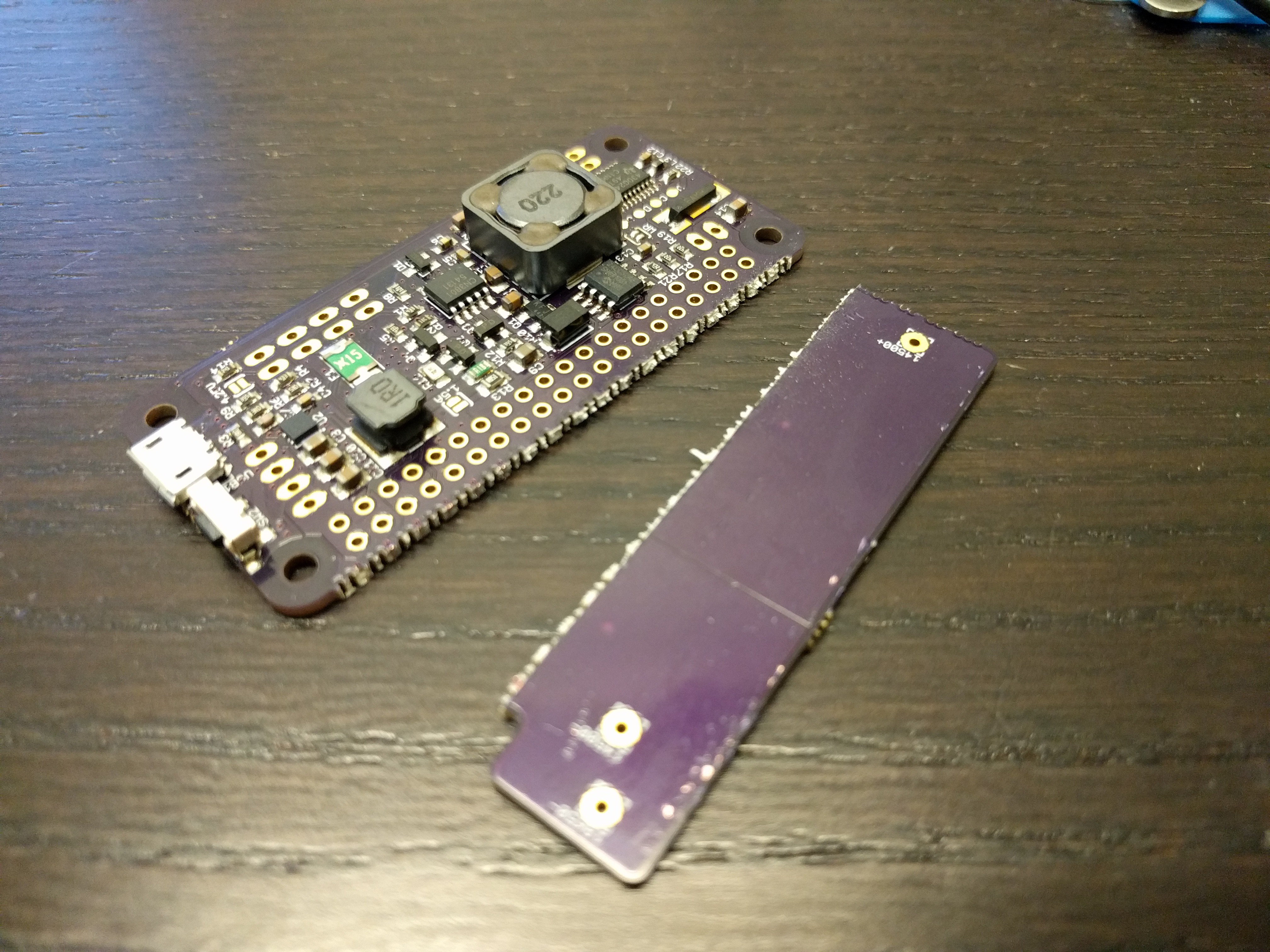
- Breaking the 18650 mounting PCB part off worked fine, breaking the complete battery holder part off was another story. I did manage to break it off, but it put way too much strain on the PCB for my liking.
![]()
So I now have added a gap that should make this process simpler. Based on demand, I may also decide to have separate panels without the battery holder for those that want to use their own LiFePO4 battery.
- I adjusted the layout around the 32kHz crystal so it now has a ground island and guard ring around the sensitive crystal signals.
- I moved the programming pads a bit farther from the inductor for easier access.
- I added some extra capacitors since ceramic capacitors have the habit of not having their full capacitance under bias voltage, and I want to make sure the supplies are clean. Victim is the 4.25V output voltage option, which nobody seemed to be asking for anyway. Yes, it would allow higher output current, but the output wattage would still be the same. Since downstream there are usually switching power supplies, the lower voltage won't change the available power.
- I changed the micro's supply ferrite beat and capacitor to a small resistor and bigger capacitor. I had observed that under light load the battery voltage had some low frequency noise on it because the boost converter goes to PFM mode, and the periodic on/off puts little dips in the supply at around 30kHz. The resistor / bigger capacitor combination will filter this better.
- The fused battery voltage output was replaced by a battery output switched by load switch. It provides protection and also turns the output on and off with the 5V output. I just was not comfortable with the concept of having people connect stuff to the battery and be responsible for not over discharging the battery. Now the LiFePO4wered/Pi+ circuitry can ensure the battery is not over discharged.
- The charger switching MOSFET was upgraded to a higher power and current device since the current one blew out at high voltage and load current. This required a new footprint.
- I still have the HAT EEPROM circuitry on the board but don't intend to populate it. The HAT standard is completely retarded in that it only allows ONE HAT, and only reads one HAT EEPROM address, even though it uses a bus. This means that if people would use a LiFePO4wered/Pi+ they could not combine it with another HAT. Since most of my customers order stackable headers, many must be using my current products with other HATs and it would be a disservice to populate the EEPROM on mine. But since the LiFePO4wered/Pi+ is intended to be a base for other products that use the full HAT size and add custom circuitry, I'm reserving the space for the EEPROM so it is available for those spin-off products.
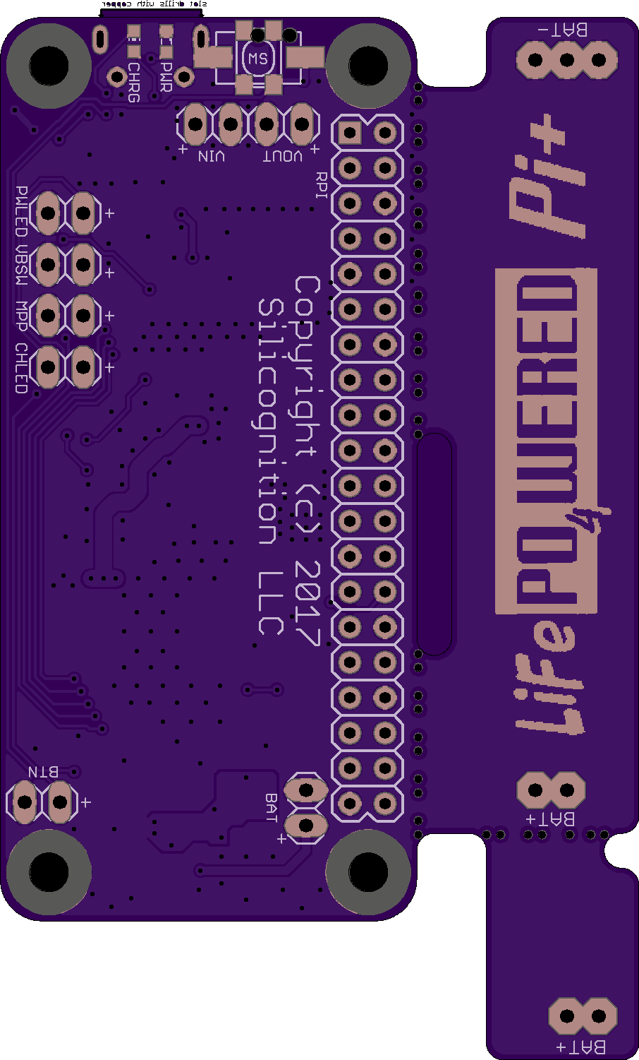
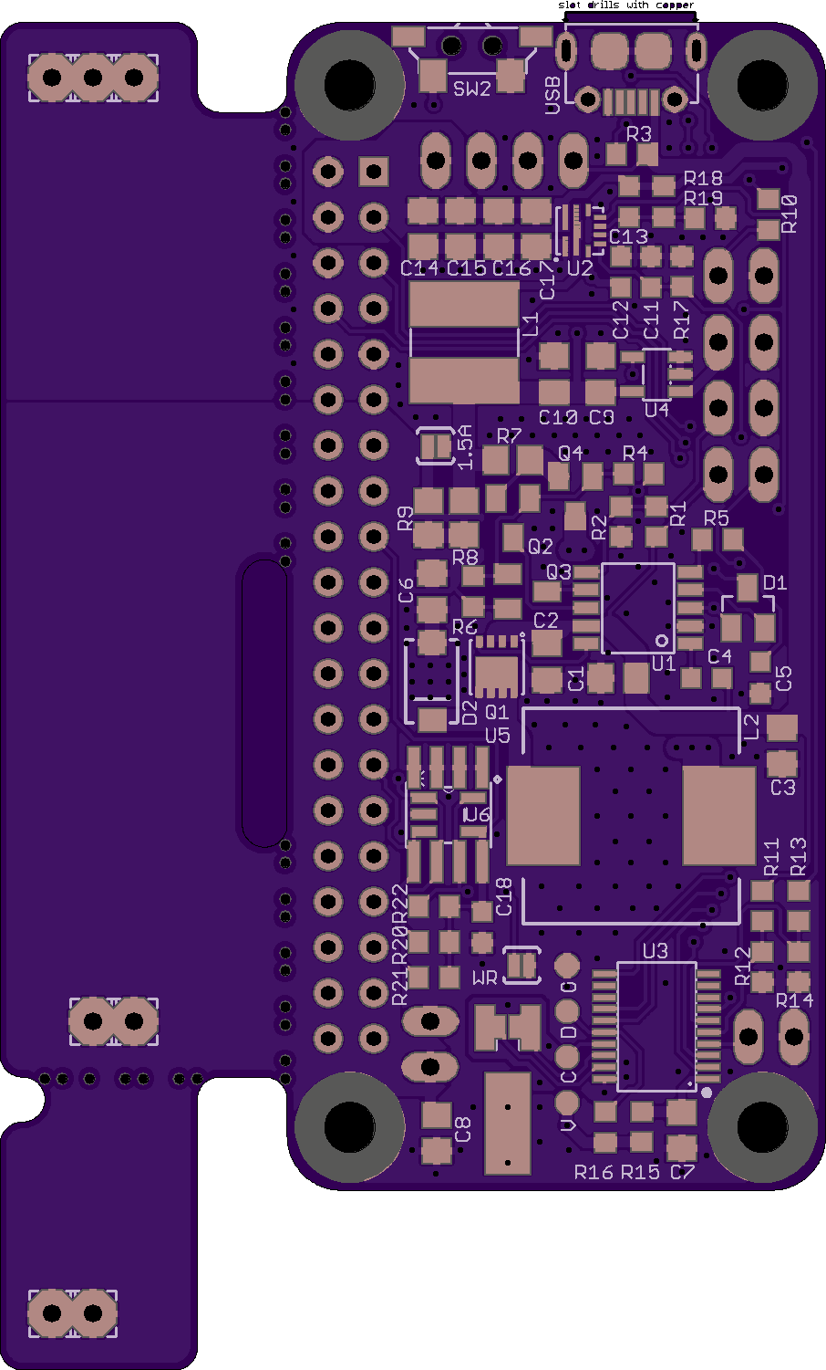
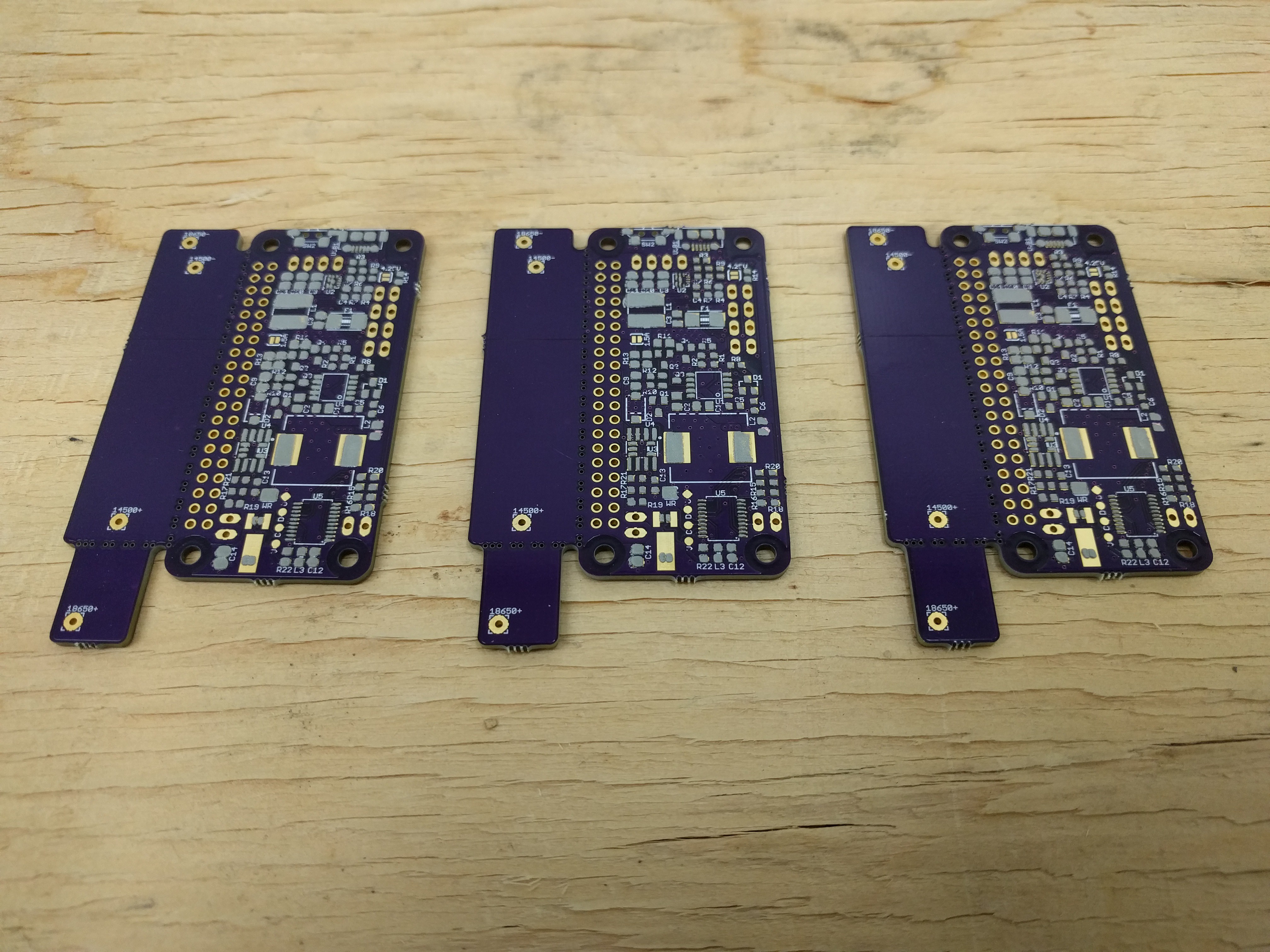
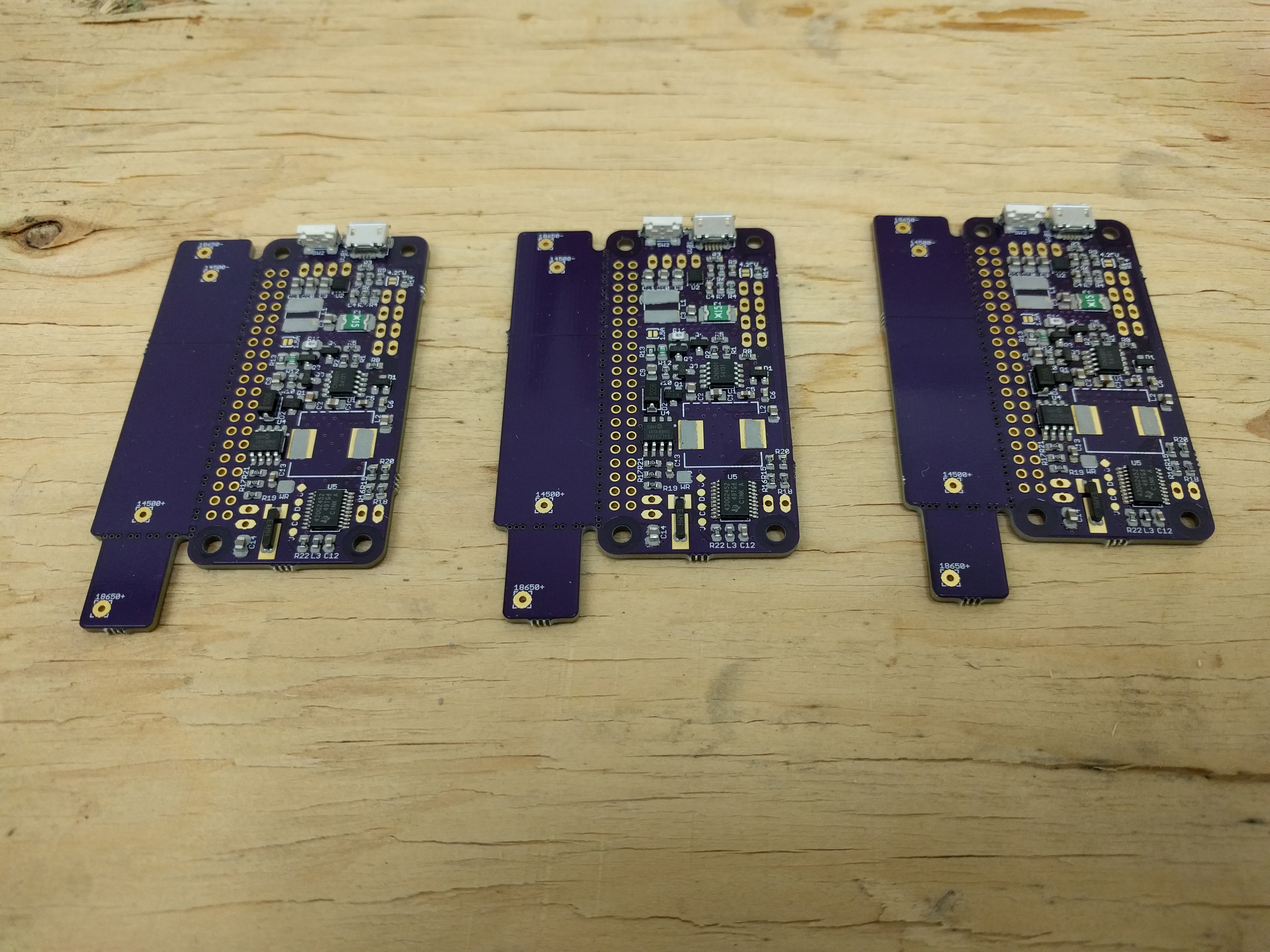
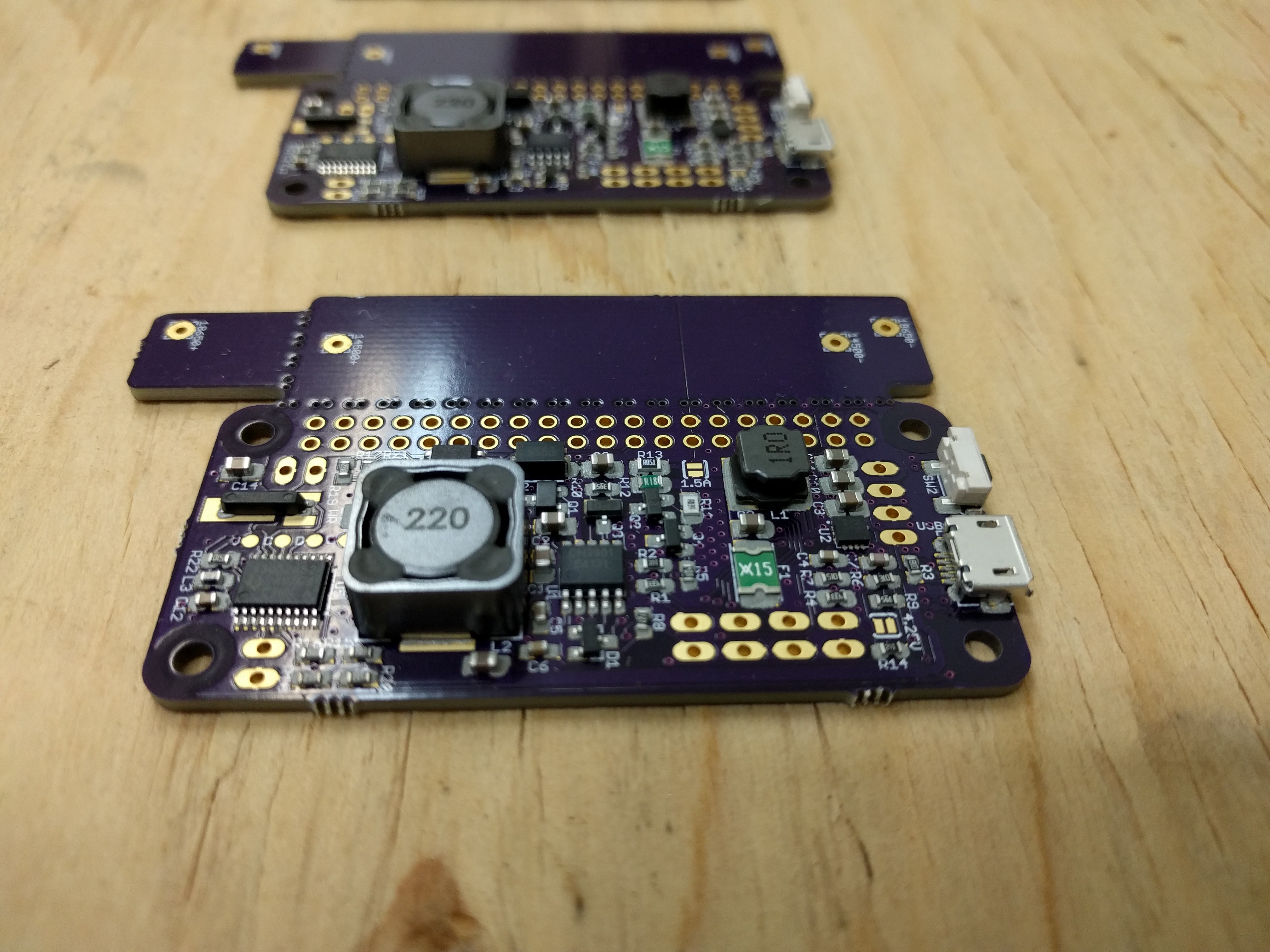
I think that's about it for significant hardware changes. Here's the new layout as sent to @oshpark :
![]()
![]()
-
Progress in learning and code
11/06/2017 at 18:29 • 1 commentI figured out some stuff since I burned up my power MOSFET last time. Stuff like: "Read the datasheet more carefully dummy"! :)
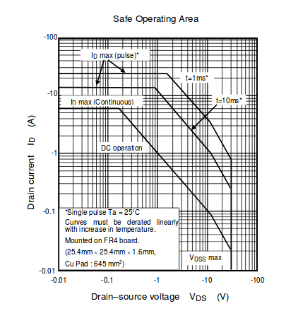
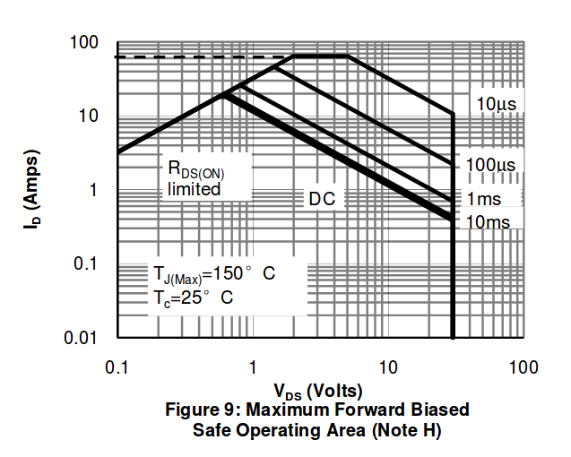
The SSM3J332R datasheet has the following graph in it:
![]()
This makes it obvious that current capability of the MOSFET is seriously reduced at higher VDS. The graph shows lines for pulse lengths but I'm not sure how repeated pulses play into this. To be safe, I'm just scaling the DC line value by the duty cycle. At 20V, that means the SSM3J332R is only rated for... about 260mA with 15% duty cycle. No wonder it burned up!
So, need to find a better MOSFET. Unfortunately that means more expensive as well. I stumbled across the AON7408, which is a significant step up and still low cost. Unfortunately it's in a DFN package, and I prefer leaded packages. But since my quest to replace the TPS61236P boost converter didn't turn up any good alternatives, I already am stuck with one DFN anyway so I might as well add another one. On the upside, there seem to be many MOSFETs available in this package so if the AON7408 doesn't work out it should be easy to find an alternative in the same footprint.
Here is the same safe operating area graph for the AON7408:
![]()
In the same conditions at 20V with 15% duty cycle, the AON7408 should be able to deal with 4A. A significant improvement, and the MOSFET fits in the same area as the original one.
This also makes me wonder if some of the heat at 20V, 2A I saw in the previous project log near the Schottky diode was actually the MOSFET starting to burn up. The resolving power of the thermal camera is just not good enough to tell where exactly the heat comes from if two components are close together. Hopefully, the overall power dissipation and heat in the system will go down with this change, since the MOSFET has significantly lower RdsON as well.
On the software side, I have finally implemented code for the 32 kHz crystal and RTC functions. It's pretty cool to see the Pi wake up at an exact time. :) I need to do some more testing, but I've started work on the next PCB revision and have started some volume component orders. Exciting! :)
-
2A load current! *
10/21/2017 at 04:16 • 2 commentsSuccess! I finally managed to get the LiFePO4wered/Pi+ to 2A continuous load current in UPS mode! :) Without active cooling, and with the charger keeping up and keeping the battery charged. So what changed?
As I have previously explained, it all comes down to limiting the heat production on the board. One commenter suggested I switch the 60V 5A SS56 Schottky diode for a lower voltage model, such as a 40V 5V SS54. The reason is that the diode drop in the forward direction is lower for a diode with lower reverse breakdown voltage. With a lower forward voltage, it will dissipate less heat. I tried that, but unfortunately it didn't seem to make much of a difference.
So I decided to look over some of my old thermal camera shots again to see what was producing the heat.
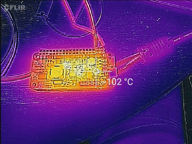
![]()
In this one I was measuring the diode temperature, but as you can tell, there's another hot spot, between the 2 and 0 of the "> 120°C" text. It even seems a little brighter than the diode spot, actually. This is transistor Q4 in the schematic, it's present (in combination with Q2 and Q3) to disconnect the charging circuit from the battery when the battery isn't charged, to minimize current leakage. Of course, while charging, it has the full charge current flowing through it. Assuming conversion from ~3V to 5V at about 90% efficiency, this transistor has a continuous current of about 3.7A flowing through it when the load draws 2A. Unfortunately the Vgs voltage is only 3V or so, so the transistor isn't turned on as hard as would be ideal, and likely has a RdsON of around 100mΩ. This results in burning 1.37W of power in this little SOT23 transistor and it gets HOT. Too hot probably, the DMG2305UX spec mentions 1.4W max mounted on 1 inch square 2 oz copper, which I'm not meeting in that location, especially since the diode is also heating the board.
So I decided to try a different transistor, a Toshiba SSM3J338R (with the original SS56 diode). It is specified to have 20mΩ typical RdsON at 2.5V Vgs, so it should be a good improvement and it has a SOT23 package as well. It should only dissipate 0.27W at the same current, resulting in 5 times less heat.
And it works! Here's a thermal shot:
![]()
And having it loaded with 2A, coming up from discharged battery, the system manages to supply the load with 2A and charge the battery, as it required for UPS functionality. Success!
But you must have noticed the little star, asterisk "*" in the heading. You know what that means. :) Fine print, exceptions, disclaimers, etc. Well there are some here as well.
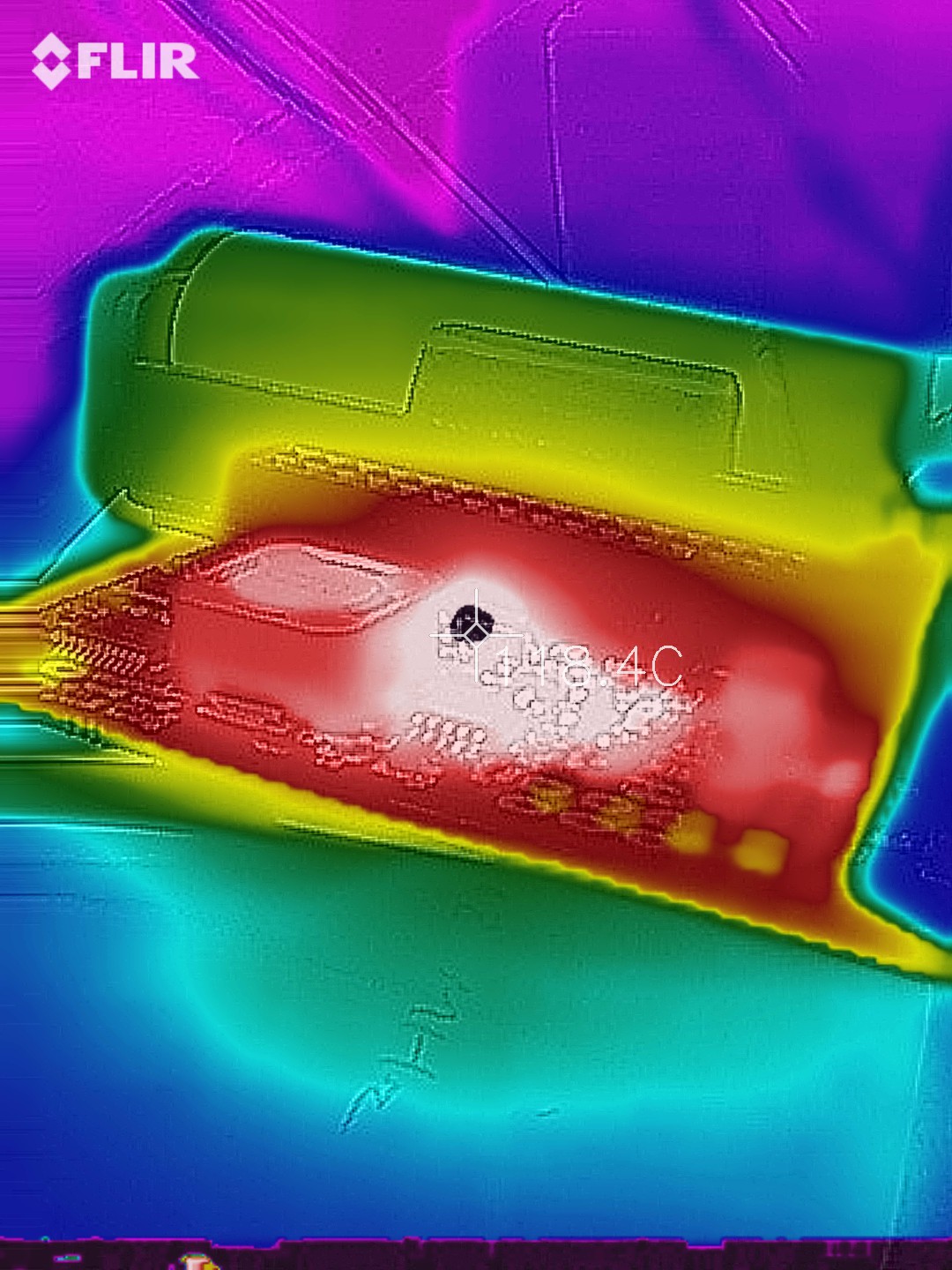
In this case, it's about the input voltage to the system. These tests were all done with 5V USB input, but I've designed the board to accept input voltages up to 24V. So I decided to test what would happen at 2A with 20V input voltage. The result isn't good:
![]()
Yikes, frying the diode again! This makes sense unfortunately. At high input voltages, the PWM duty cycle is very low, which means that current is most of the time flowing through the freewheel diode. At 5V input, the diode only conducts around 40% of the time, but at 20V input it's about 85% of the time.
Every power system is subject to trade-offs like this. I'm all right with lower current capability when powered by higher input voltages--it's a trade-off the customer will have to make in their system design. As long as it can do 2A with 5V input I'm happy.
So how low do we need to go to have it work as a UPS and not overheat? i tried 1.5A load:
![]()
Better, "only" 110°C, but still too hot, since the battery discharges while plugged in.
Ok, try 1A then:
![]()
That's better, only 82°C and the system stays cool enough to allow the battery to charge! It's not 2A, but it still can act as a UPS for a Pi3 at 100% CPU.
Then I wondered: since at the higher input voltage the diode becomes the problem again, maybe switching to the lower voltage SS54 would be helpful to reduce heat in this condition?
So I tried 1A load with both the SS54 and SSM3J338R:
![]()
Great, that reduced it to 74°C. Maybe we can try higher current now? Bump it back up to 1.5A:
![]()
Hmm, hot. The reading is higher than with the other diode actually. Oddly, the battery IS charging with this load. I guess maybe I measured temperature in a slightly different spot? All I know is that it is charging the battery and it would work as a UPS with 1.5A load and 20V input voltage. Awesome!
So how about 2A? I bumped it up and waited for the system to settle to take another picture. That's when I heard a faint sizzle, and when I looked at the board, I saw magic smoke and a little flame! :$
So, here's the last picture showing the damage:
![]()
Oddly it's switching transistor Q1, a Toshiba SSM3J332R, that has bitten the dust. That's not what I expected since at high input voltages, this transistor is on LESS, only about 15% of the time at 20V input, so it seems it would take less of a beating.
I'll need to figure out why that happened. My guess is that with the low duty cycle, the peak current is going to be significantly higher than the average current, much higher than at more moderate duty cycles at lower voltages. Anyone have any insights that could help me?
In summary, this is why we make prototypes. :) A lot to learn as usual. I'm feeling confident we're getting closer to figuring it all out, and production.
-
ETA1096 evaluation
10/18/2017 at 17:31 • 0 commentsIn my quest to reduce the cost and manufacturability of the LiFePO4wered/Pi+, my attention was drawn to the ETA1096, a Chinese boost converter. It is significantly lower cost than the TPS61236P, and it comes in a nice leaded package, so I thought I'd evaluate it to see if I could use it on the LiFePO4wered/Pi+.
I found out about this part while investigating some of my competitors. I found the Geekworm UPS HAT and although the creator tries very hard to hide which parts are used by scraping the surface markings off, some smart people on the internet figured it out anyway. Since the UPS lists 2A output current and the chip's specification lists up to 3A, it looked promising.
What was harder was to get a hold of samples to evaluate. The Chinese distributor refused to ship samples in the mail, and I wasn't going to spend $100+ to have a couple cheap chips shipped by Fedex. In the end I decided that the cheapest way to get a sample part was to buy the Geekworm UPS HAT. :)
Now it might be considered a stupid idea for my business to talk about a competitor here, but honestly the Geekworm UPS HAT is a pretty lousy device compared to the LiFePO4wered/Pi and Pi+. Of course I'm biased, but check out this attempt by an enterprising individual to make it usable and you'll know what I mean. Calling it a UPS is a bit of a stretch in my opinion, the out-of-the-box functionality is really limited. It's something you can make usable if you want a project, but if you just want something that works so you can get on with the project you're already doing, you might want to get a LiFePO4wered/Pi instead. ;)
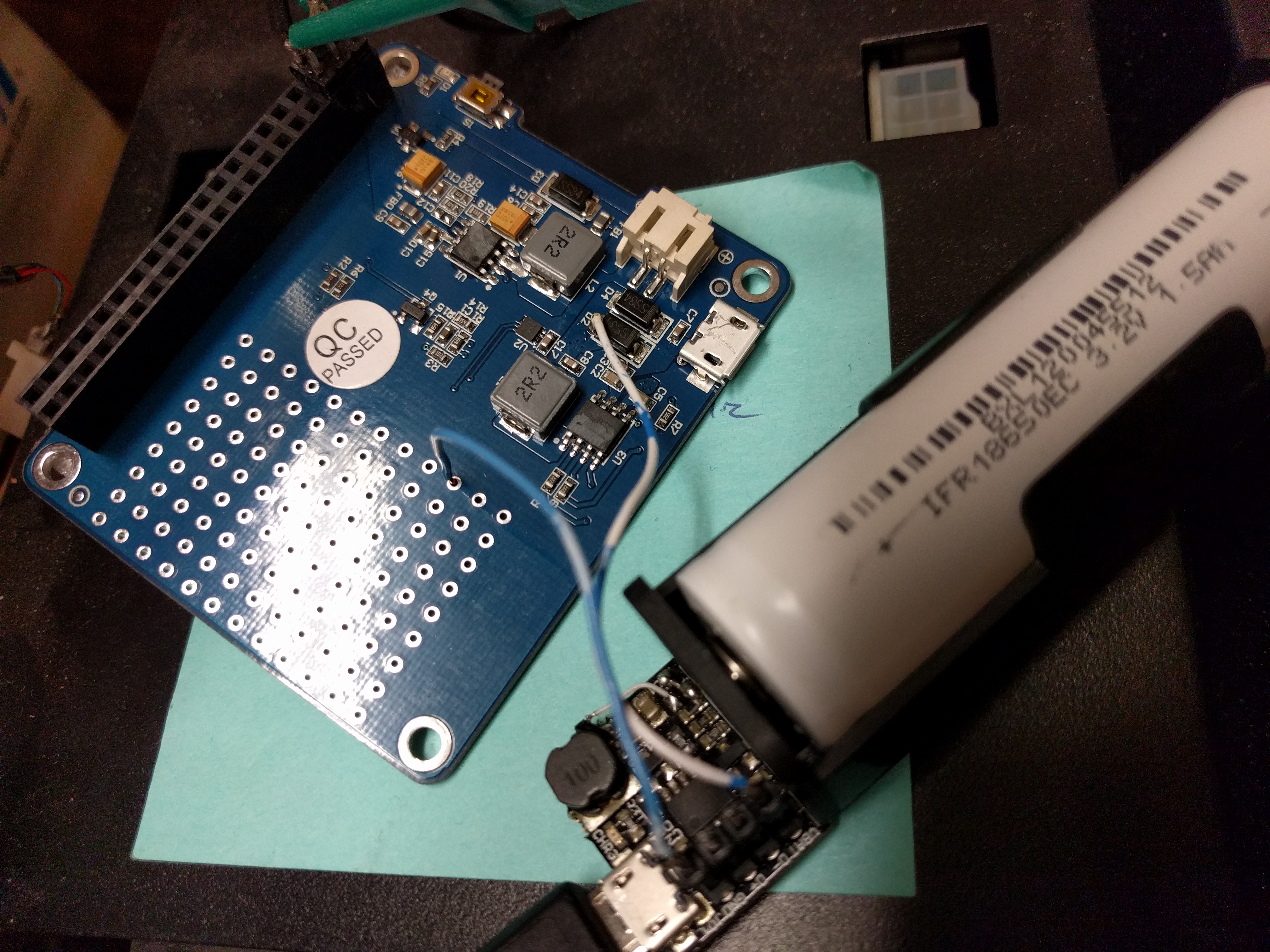
I decided to hack in my own battery and charger (a #LiFePO4wered/18650 base) so I could focus on the ETA1096 performance without worrying about the rest of the system.
![]()
[Just one quick note on the "rest of the system". The charger chip (likely an ETA9741) is an odd part that actually puts 5V back on the input USB port even if the ETA1096 is off, and seems to draw 40-200uA from the battery.]
I used my electronic load and started with a load current of 1A. The ETA1096 seemed to be doing fine, the voltage didn't sag and the chip didn't seem to get warm. I bumped the current to 2A and the whole thing shut off. OK... start over and take smaller steps I guess?
So I went to 1.1A, 1.2A, 1.3A, 1.4A, 1.5A, 1.6A and it shut off again. Start over and let's keep it at 1.5A. After a minute I decided to touch the chip to check how hot it was and I yelped--blazing hot! I don't have access to the thermal camera at the moment so I used my IR thermometer and it reported 107°C! And it's always been conservative compared to the FLIR One since it averages a larger area.
Well, that's... unexpected. I knew it would get warmer than the TPS61236P since it has 40/55 mΩ MOSFETs instead of the TPS61236P's 14/14 mΩ. But that still only translates into 0.3W instead of 0.1W (based on 2.8A switch current estimate due to 3V->5V @ ~90% efficiency guess), not the "blazing hot" I was getting.
I guess I'll forget about the ETA1096 and stick to the "expensive" TPS61236P for now. ;) It bugs me though that I don't quite understand what's going on and cannot explain the amount of heat produced. I seem to be missing something and would love some fresh ideas on what might be happening.
-
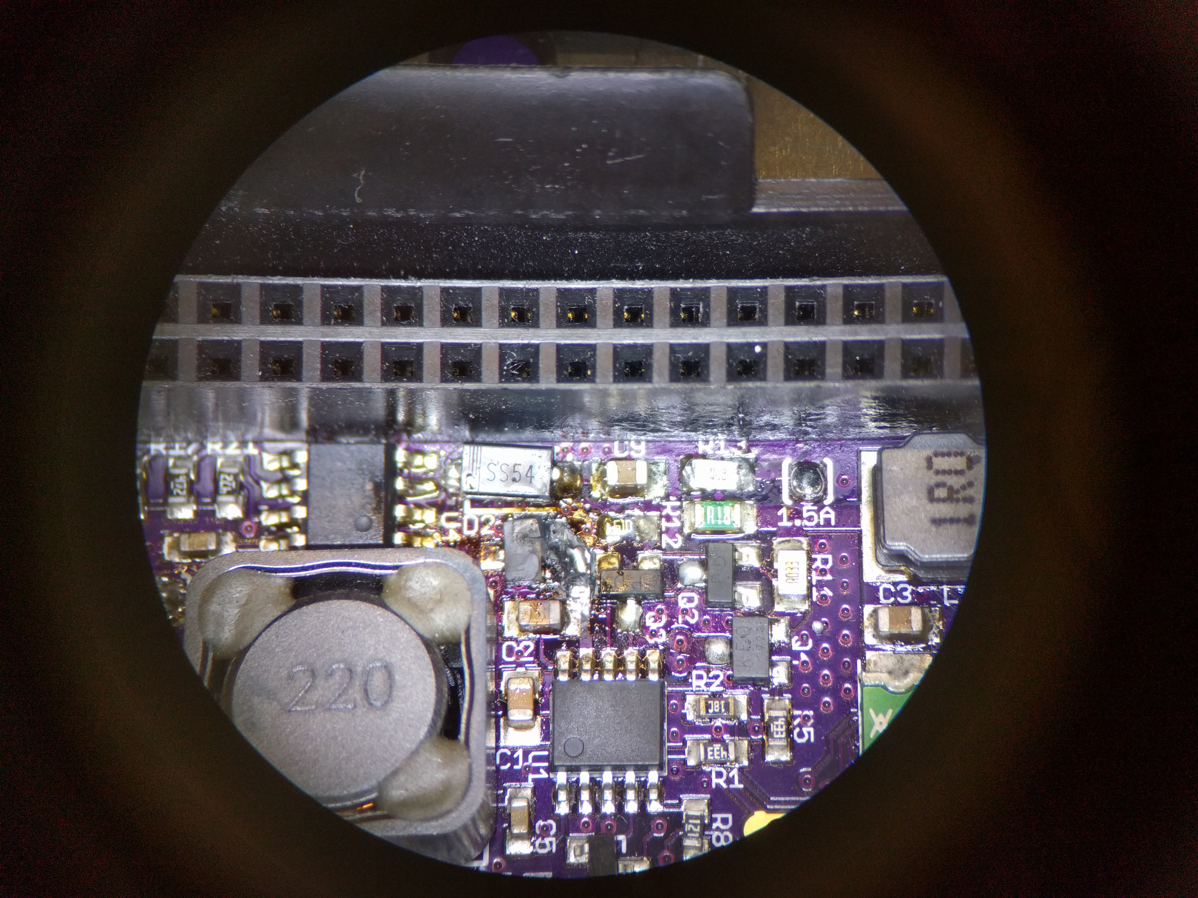
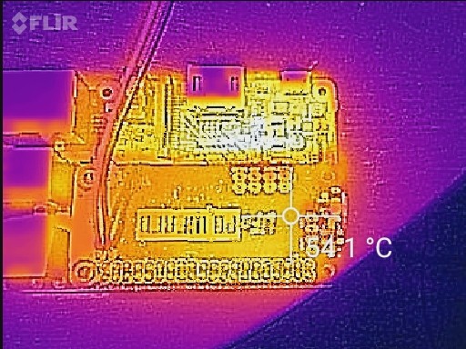
Current sense bypass check
08/16/2017 at 22:42 • 0 commentsOne concern I had was that when using the small 14500 size battery, the current sense resistor that limits the charge current also is in series with the load when running from the battery. My concern was that it would drop so much voltage that the software would decide that the battery was depleted and shut down. This is, of course, not a problem since the battery voltage is measured directly at the battery, and not after the sense resistor. But I had temporarily forgotten that. :)
So I did a test where I used a MOSFET to bypass the 0.18 ohm resistor when the input (charge) voltage was not present. I wanted to see if it affected run time from the small battery. This is still a valid test, because the boost converter does see lower input voltage due to the voltage drop across the sense resistor, so its efficiency might go down.
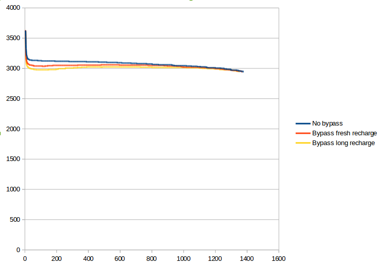
The test was done with a Pi3 with 4 cores @ 100% and an active SSH connection over WiFi. Here are graphs of the battery voltage in mV:
![]()
Oddly, the results look better without the bypass. The worst result was after a recharge a day ago, the voltage would droop and threaten to fall below the shutdown threshold, but then recovered. The longest run time is without any bypass, and was about 23 minutes.
I don't know for sure what caused the initial droop, it could be a chemical effect in the battery when charging wasn't recent and ion mobility may be lower. I will have to do a little more testing on that since it comes dangerously close to the shutdown threshold.
Overall this is good, the little battery did hold up so it's promising as a solution for those who are looking for UPS functionality and just want enough power to get through a clean shutdown. The Pi was pulling ~950mA at 5V, which translates to about 1.6A at the battery voltage. Testing with my electronic load seems to indicate 1.2A output current is the limit for the small cell, at which point the boost converter output droops to ~4.85V, still within the USB spec.
-
Getting to 2A... or not
08/10/2017 at 23:43 • 2 commentsIn trying to get to my goal of 2A output power, I've run into my old nemesis again: heat. After getting stable operation at 1.8A continuous output current, I thought I could get to 2A with minimal effort just by changing some current sense resistors. But this doesn't seem to be the case.
The main culprit is the asynchronous charger's Schottky diode. For all other power components, it's pretty much up to me how much heat they generate. If it gets too hot, just get a MOSFET with lower RdsON, or an inductor with lower resistance etc. But for the Schottky diode, it's another story. Sure, you can get a diode in a larger package, allowing it to dissipate more power safely, but it's still going to generate the same amount of heat, because due to physics the diode will always drop voltage. So it will always dissipate power (P=V*I). Worse, the amount of voltage it drops goes up with higher current as well.
Now 2A doesn't seem to be that much current, but keep in mind that I'm aiming for 2A output current at 5V, which means that with a battery voltage of minimum 3V, and counting on converter efficiency around 85%, the diode sees average currents of (2A*5V)/(3V*0.85)=3.9A. Now I understand why, even though the power components are external, the CN3801 datasheet indicates 4A maximum output current. How much power is dissipated? At 4A, the SS56 Schottky diode I use drops around 0.6V, burning off 2.4W. As it gets hot, it starts to exhibit an appreciable reverse current as well, leading to even more losses.
The mechanism preventing me from getting to 2A due to this heat seems to work like this: as the circuit (mostly the diode) heats up, some of this heat warms up the CN3801, eventually at high temperatures making the current sense voltage reference drop. Nominally 120mV, I've seen it go as low as 95mV when drawing high currents. This will in turn limit the amount of current drawn (for the same sense resistor, lower current will generate this lower sense voltage). So the whole thing is self-limiting: as it gets hot, it will limit the current. This could be considered a feature I guess, but the bottom line is that even when you lower the sense resistor, as things get hot the sense voltage drops enough to negate the lower sense resistor.
I've been considering possible solutions and what this means for the project:
- Is there a way to turn this into a synchronous converter (replace Schottky diode by MOSFET) with some clever circuitry and if so, how much circuitry and will it fit? The chip has no complementary output for this so it will have to be a hack.
- My simple topology of running all current through the charger is showing its limits. Another topology would be to only run the charge current through the charger and provide a parallel path for the load current directly from the power input. Downside is that now the 5V converter needs to become step-up/step-down, since the input voltage can be as high as 24V and the battery voltage as low as 3V and both need to convert to 5V. A step-up/step-down immediately pushes you into chips that are in the several-dollar range.
- A spec fix: instead of 2A max, advertise the system as 1.8A max. The heat still bugs me, and will limit the current even lower at higher temperature. 2A is also a nicer number, and what the Raspberry Pi foundation recommends for a Pi3 power supply. On the other hand, 1.8A is double what the current #LiFePO4wered/Pi3 can do without active cooling, so it's still a pretty nice upgrade.
I would very much like user feedback on this. How much current do you need? The current design works well at 1.8A, and can probably go into production this fall. Completely changing the topology will get me past 2A, but is a big redesign that will likely not reach production this year. Would it be worth it to delay and get the spec I wanted? It would likely also conflict with other goals such as making it cheaper...
-
Load test results
06/22/2017 at 23:40 • 1 commentFinally got around to doing some serious testing, and overall the results are looking good!
I used a prototype with the battery holder area broken off and an external battery connected. This configuration has the smallest PCB copper area, and as such will have the worst thermal performance. I tested with a Pi3 @ 100% CPU first to get a baseline. This first thermal shot is running from the battery without charging:
![]()
Very good, doesn't get hot at all even though the Pi is cooking!
Now a shot while also charging the battery:
![]()
The hot spot is hotter and has shifted to the charging area, which makes sense. The charger is an asynchronous step-down design, which is less efficient than the synchronous boost converter.
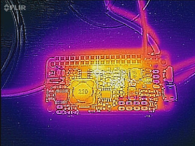
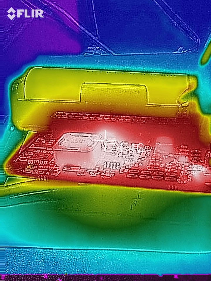
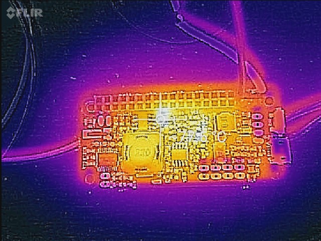
To be able to see the components (which are on the bottom, facing the Pi), at this point I decided to switch to my electronic load instead. First I ran the system at a load of 1A, similar to a Pi3 at 100% CPU:
![]()
As expected, the culprit is the asynchronous charger's Schottky diode. Unfortunately, the diode will always drop a voltage, so it will always dissipate heat. Because I anticipated this, I put a ton of vias around the diode to try and pull as much of this heat as possible to the top side ground plane. As the images show there's only a few degrees C difference between the diode temperature and the temperature measured on the top side, so this seems to be doing the trick. My prototype PCBs only use 1 oz copper as well, for production I intend to use 2 oz copper instead which should increase the heat sinking capability of the ground plane.
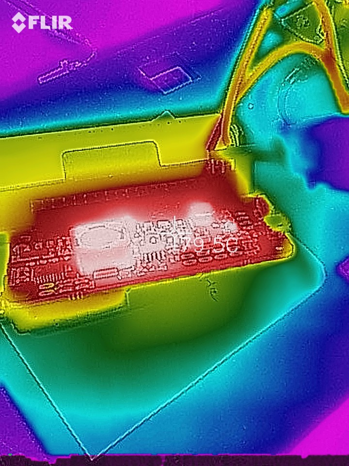
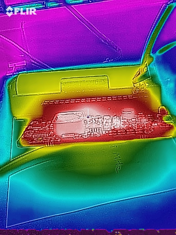
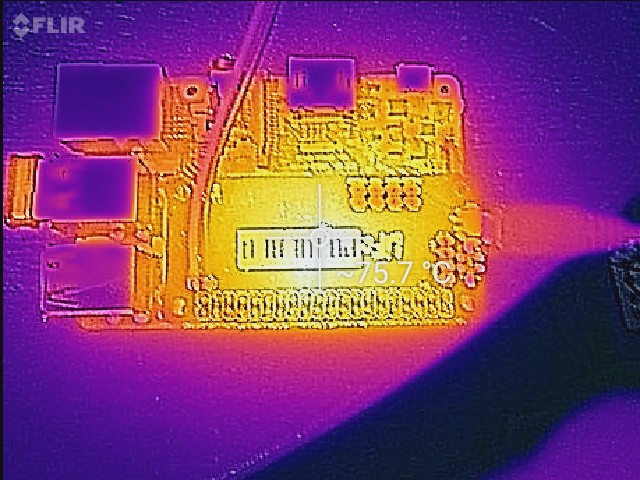
Next I wanted to see what would happen if I really loaded this puppy. I cranked up the electronic load to 2.5A. I only designed the system for 2A loads, but I like to be mean during testing to make sure things aren't marginal.
![]()
Ouch, hot! Unfortunately the FLIR camera can't seem to measure hotter than 120C, so I don't know how hot the diode actually is. On the plus side, the diode is rated for 150C, and I had it running for several days like this without anything going up in smoke. :)
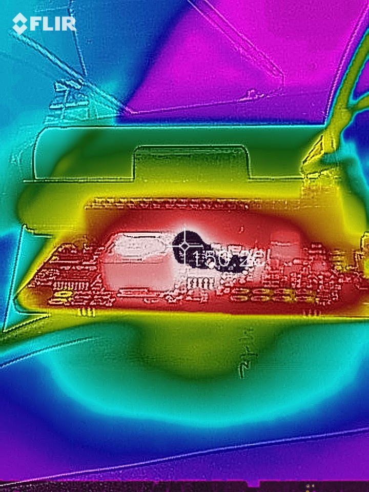
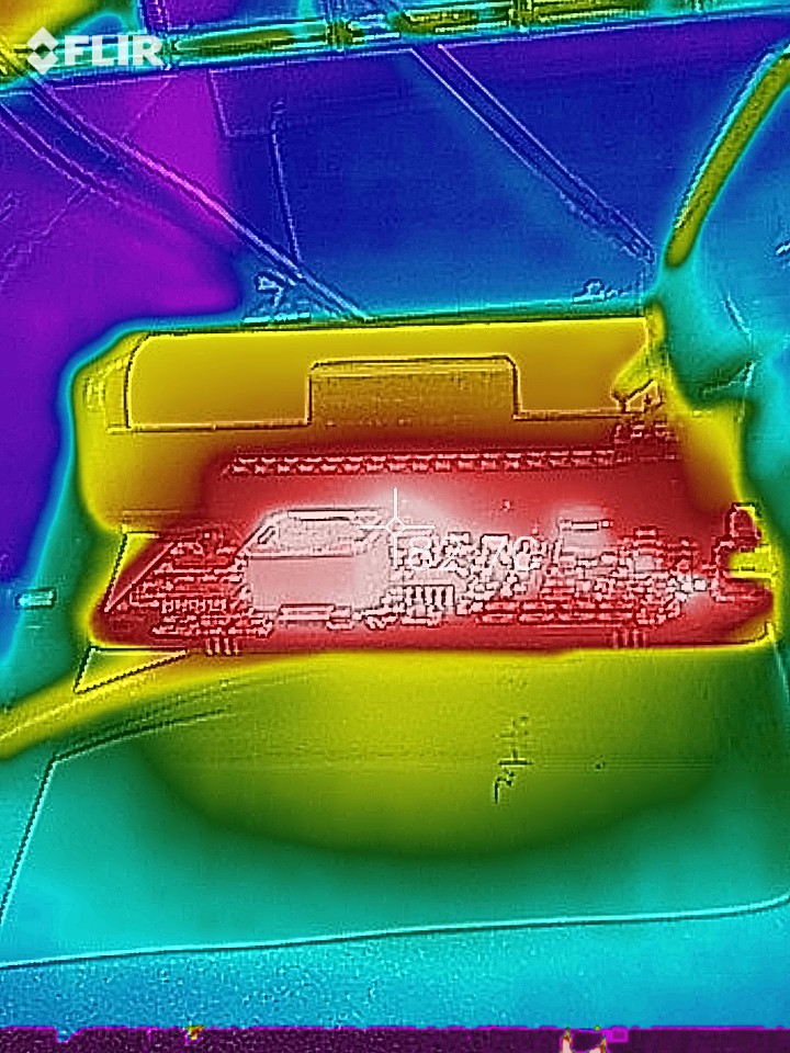
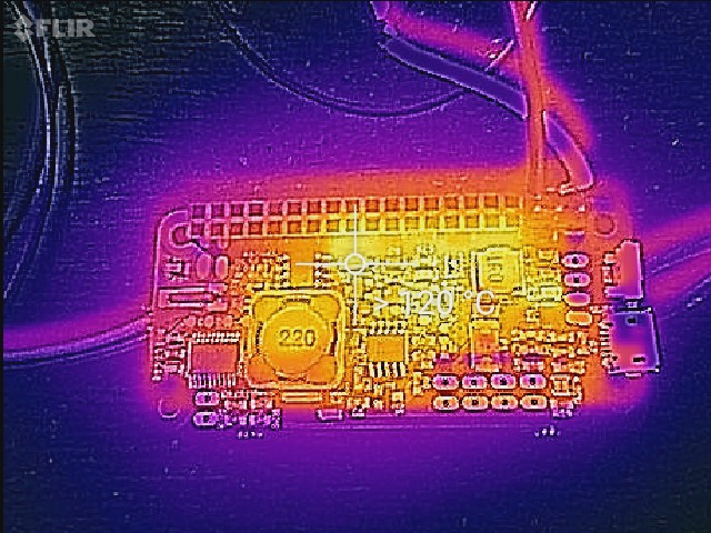
The boost converter got pretty hot too at this load:
![]()
As this chip is rated up to 125C, I don't think this is something to worry about at this point. If the system is going to be used at high load and elevated ambient temperature, more thermal management will have to be added. I intend to do some future tests with a heat sink on top of the PCB as well.
On the low power side, the system is pulling 3-4 uA from the battery with the Pi off, so it seems my scheme to disconnect the charger from the battery when not charging is working as well.
I tried to run at high load continuously but I ran into an issue with that. I would try to run overnight but would find the system off in the morning. I finally figured out the charging chip was regulating to a lowish 104 mV across the current sense instead of 120 mV. So the system was discharging the battery instead of charging it. I had to lower the load to 1.8A to keep the battery charging. This means that I need to make some adjustments in the current sense resistors to account for tolerances due to temperature etc and still reliably charge the battery at 2A load.
-
It's alive!
05/19/2017 at 23:35 • 0 commentsAfter hacking on firmware for the past two weeks, I'm happy to report that the prototypes are working!
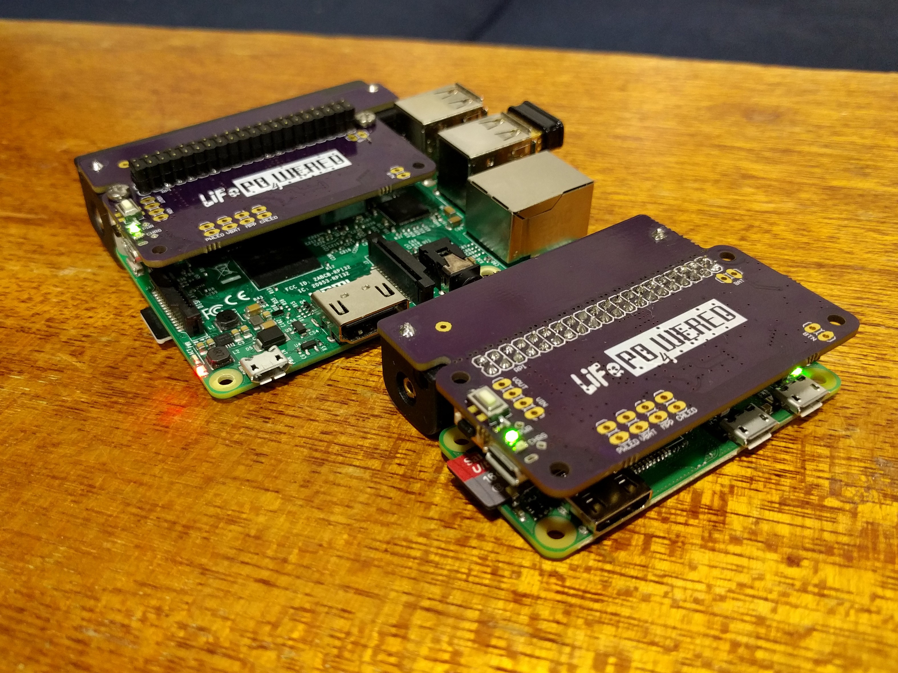
Here are my two protos: running a Pi 3 and a Pi Zero W:
![]()
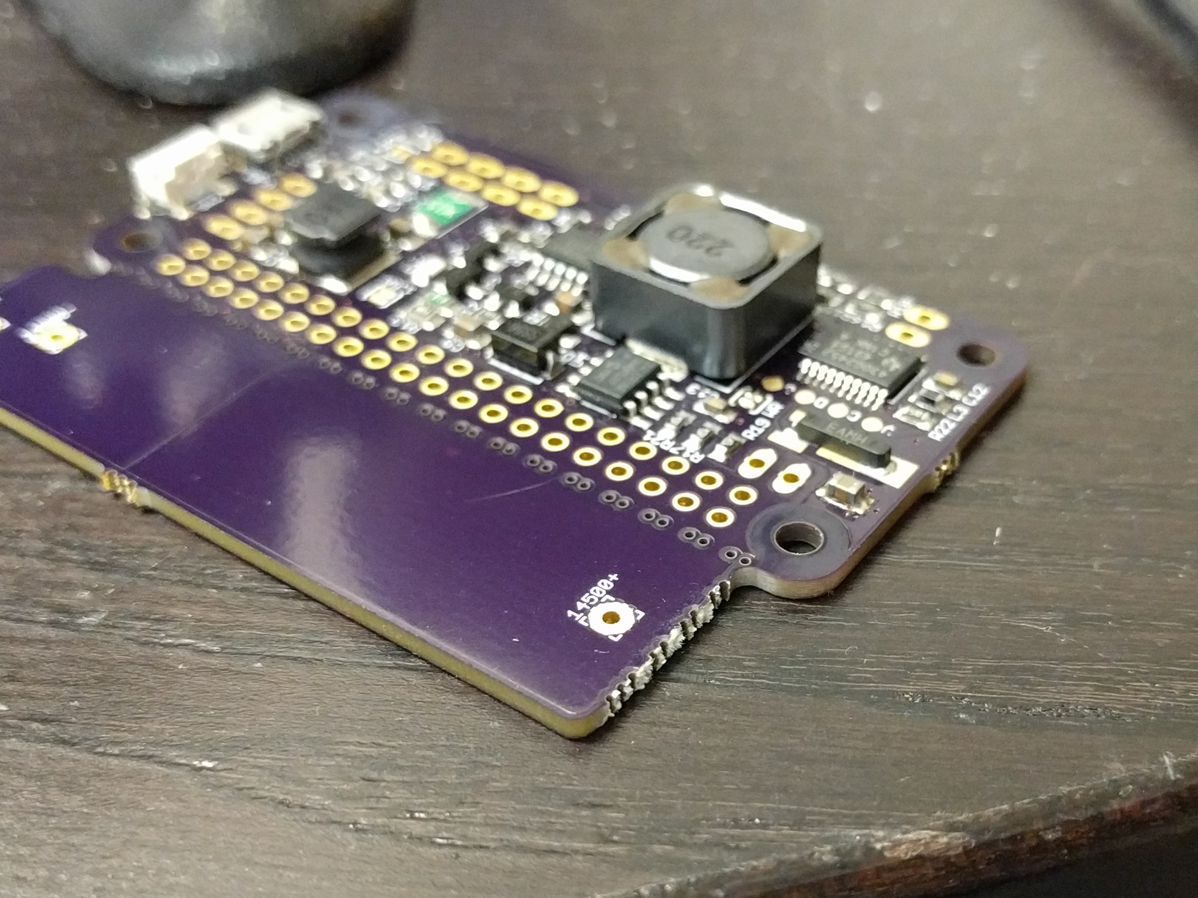
The prototype in the back uses a 18650 LiFePO4 battery and stackable header, the one in the front uses a 14500 (AA) LiFePO4 battery and normal header. To remove the excess PCB used for the bigger battery from the unit with the smaller battery, I had added perforations to the PCB, but I was worried that the copper foil might peel when breaking it off. I decided to see what would happen with and without scoring with a knife, so I scored only part of the perforated area. Here's the result:
![]()
The section of PCB broke off very clean, and I honestly cannot see any difference between the part that I had scored and the part that I hadn't. Very good news! I'll have to see what happens when breaking off the bigger section when I'm ready to build a prototype with external battery.
On the firmware side, I worked on the following:
- Different pin assignments since I had to switch to a 20-pin package to accommodate an extra signal and had run out of pins.
- The extra signal allows measuring the Raspberry Pi current consumption.
- Separate single point calibration values for VIN, VBAT, VOUT and IOUT instead of a single calibration value based on VBAT. Since the range of VIN is now huge (24V) compared to the range of VBAT (5V), the single calibration value wasn't working well.
- Added shadow buffering to the I2C driver. This allows atomic read and write of multi-byte values to prevent race conditions, and will be very important when implementing RTC functionality.
- Timeouts for boot and shutdown phases. At the moment they are hard coded to 5 minutes for boot and 2 minutes for shutdown, but the idea is that they will be settable in 10 s increments. This improves behavior when the Pi is not present or unresponsive.
- Support for mechanical switch (default for LiFePO4wered/Pi+) in addition to capacitive touch. As you can see in the pictures, the prototypes have a side-facing switch as well as a top-facing one. The side-facing will likely be standard and the top-facing an option. There are also pads to connect an external button or cap touch pad.
- Improvements to reduce power consumption when off (still monitoring voltages and button), around 3uA now. Initially I had a problem where the current was ~80uA if the Pi wasn't connected.
Once functional, I could do some preliminary testing, and things look promising:
- With a Pi 3 running at 100% on 4 cores (~950 mA), the board was warm but not hot. This is promising for extra power capability!
- The split sense resistor scheme to allow much higher load current than charge current seems to work! The prototype with the small battery was able to power a Pi 3 @ 100% while also charging the battery quickly, but not above its rating when under low load.
- The 40-pin header with 2 screws seems to be mechanically solid.
Next I'll need to do more detailed high-power testing to see where the limits are. I still need to add registers to set the boot and shutdown timeouts and implement RTC functionality.
-
First prototype build
05/08/2017 at 23:53 • 0 commentsI decided to build up my first prototypes of the LiFePO4wered/Pi+ today. Since I wanted to do all 3 boards I received from OSH Park, and there are quite a lot of components, I figured using solder paste and reflow was the way to go instead of manual soldering.
I had not ordered a stencil so I used the laser cutter at the Tinkermill to cut my own stencil from plastic film. It never turns out as well as the professional ones you can buy, but it's free and usable. :) Below is a picture of the stencil over a bare PCB:
![]()
Time to apply solder paste:
![]()
The result with the stencil removed is fairly decent, even for the tiny and weird TPS61236P boost converter pads:
![]()
I decided to paste all 3 boards and then build them up in batch:
![]()
The disadvantage of doing this is that the paste tends to dry out during the long build. Placing the components took around 2 hours and the paste was definitely getting dry, but it seems to have had no ill effect. Here are the boards with all components placed except the inductors:
![]()
And here's a closer shot, ready to go into the reflow oven:
![]()
Here's the first board after reflow:
![]()
Looking good! :) Even the TPS61236P connections seem to have soldered fine. I was a little worried because the stencil wasn't exactly accurate for those tiny pads.
Here are all three boards done:
![]()
I still need to add the LEDs on the other side of the boards, and maybe a top button. As you can see, there is a side-facing button already on the boards but I want to evaluate different options such as side-facing and up-facing. I also need to add the 40-pin GPIO headers and battery holders.
Then I need to take the existing #LiFePO4wered/Pi firmware package and port it to this new platform. This new design needed more pins than were available on the micro I was using before, so I'm using a different part from the same family and some pin assignments have changed. Plus, I need the firmware to sample a physical button instead of a touch button and use the 32kHz crystal instead of the internal RC oscillator.
-
First prototype layout
04/17/2017 at 23:49 • 0 commentsMy prototype layout is done!
![]()
Some OSH Park renderings below:
![]()
![]()
All in all I'm pleased with the result. It was harder than expected to cram it all in, especially the larger (higher current + lower cost) inductors take up a lot of space. This board has the following features:
- Micro USB or through hole 0.1" connections for VIN. Voltages up to 15V should be supported, making it possible to hopefully power this directly from 12V car power or a <15V Voc solar panel.
- Footprint for 3 types of tactile buttons, two on top and one side facing. The idea is to evaluate different button options (only one would be populated). There are also 0.1" connections for an external button. The firmware will likely still support capacitive touch for the external button, but not on the PCB itself, and a mechanical button will be the default. This will likely reduce quiescent current as well below the current <4uA.
- The charge and power LED are right by the micro USB and button, making the user interface nice and concentrated on one side. There are also 0.1" connections to connect external LEDs if desired.
- MPP voltage is adjustable by adding a resistor to the 0.1" MPP connections. 4.65V by default for USB use, but if you use solar you can customize this now.
- Switched 5V output to the Pi (hopefully 2A+) is also available on 0.1" connections to drive external load like a screen.
- The PCB has break-off areas to accommodate either a 14500 (AA) or a 18650 size battery holder, or they can be broken off completely and a battery can be attached to 0.1" connections. Without the battery holder extensions, the PCB is Pi Zero size. The break-off quality is not tested yet and to be evaluated.
- A solder jumper is available to configure either 0.55A (14500 battery) or 1.5A (18650 battery) charge current. The current sense resistor is split to try and implement the higher-load-than-charge current system described in the previous log.
- A solder jumper is available to reduce the output voltage from 5V to 4.25V. The Pi and many peripherals can run at lower voltage and it makes the power system (on both the LiFePO4wered/Pi+ and Raspberry Pi) more efficient.
- An external 0.1" connection for VBAT is available for loads through a 1.5A resettable fuse, but if you use this you need to make sure to manage low battery conditions yourself and draw very little power when the system is off! If loads connected to this are switched from Pi GPIO outputs, it should be fine because they should turn off when the Pi is turned off. But mind the quiescent current, discharging the battery too much will kill it!
- With the new boost converter it should be possible to measure the 5V load current to the Pi and read it over I2C!
- Footprints for several types of 32kHz crystal are present, to implement RTC functionality.
- An EEPROM is present to implement the HAT spec! (Although the physical shape still won't meet the spec.) Hopefully this will result in easier software setup in the future.
LiFePO4wered/Pi+
Next Gen LiFePO4 battery / UPS / power manager for Raspberry Pi, ideal for headless and IoT use