0%
0%
Lacey Mk I
A Homebrew 68k Computer for Shits & Giggles
 Matt Lacey
Become a Hackaday.io member
Already have an account? Log in.
Just one more thing
To make the experience fit your profile, pick a username and tell us what interests you.
Pick an awesome username
hackaday.io/
Your profile's URL: hackaday.io/username. Max 25 alphanumeric characters.
Pick a few interests
Projects that share your interests
People that share your interests


 Hayden Kroepfl
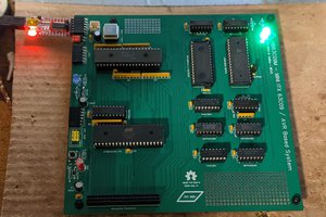
 Dave Collins
 Tony Robinson
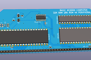
 Gee Bartlett