0%
0%
GPN17Badge::HiFi-Bodge
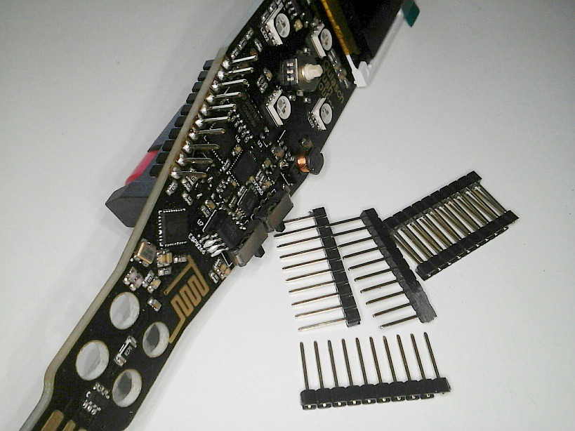
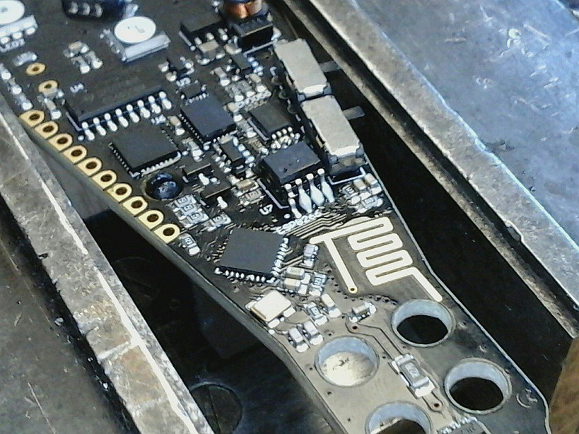
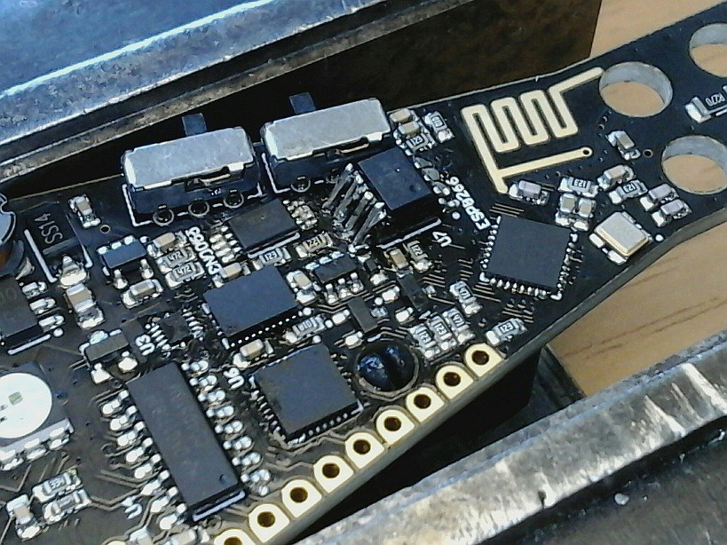
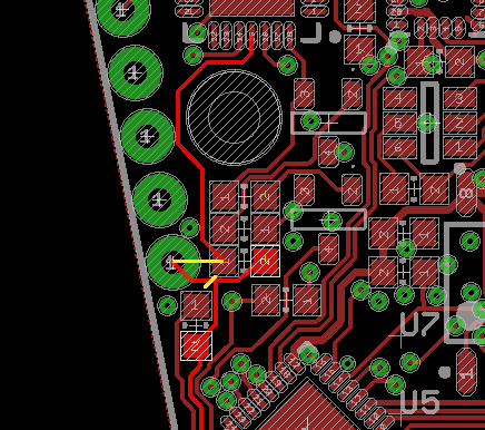
Adding high quality stereo audio to the GPN badge
 helge
helgeBecome a Hackaday.io member
Already have an account? Log in.
Just one more thing
To make the experience fit your profile, pick a username and tell us what interests you.
Pick an awesome username
hackaday.io/
Your profile's URL: hackaday.io/username. Max 25 alphanumeric characters.
Pick a few interests
Projects that share your interests
People that share your interests
 deʃhipu
 Michael O'Brien
 sapir
sapir