 helge
helgeI've made the a-priori list of modifications to get this bodge working:
I2C is routed to the DAC via the extension header. Works for me.
SPI SRAM: spiram.c says the following about the choice of peripheral chip select:
//select HSPI CS2 ,disable HSPI CS0 and CS1
CLEAR_PERI_REG_MASK(SPI_PIN(HSPI), SPI_CS2_DIS);
SET_PERI_REG_MASK(SPI_PIN(HSPI), SPI_CS0_DIS |SPI_CS1_DIS);
but SPI_CS1 and SPI_CS0 are interchangeable and all hardware chip select pins should be shared among the SPI transceivers. With GPIO0 already taken, the next best thing (and the only remaining one) is SPI_CS1 on GPIO1 / U0TXD. the CS might have to be or-ed with an output expander level to block SRAM after start-up and in config mode - it may also be hooked to the RX side of the usb serial chip so it can be driven high by an I2C slave chip on the add-on board as long as the 470R * SRAM CS input capacitance time constant penalty does not mess up SPI timing.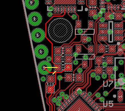
LCD:
now it gets dirty. The display gets its own SPI channel to profit from DMA. Otherwise high frame rates wouldn't be possible. This lends itself to occupying a dedicated chip select pin. The display controller ILI9163C accepts a stream of frames and once initiated, it does not need CS interaction, allowing the LCD CS to be bit banged at the start of a new frame. I've seen the display glitch and stop updating, so maybe "only once" is not the best idea. Bit-banged CS toggle (low-high-low) to initiate a frame transfer seems legit.
GPIO15is not easy to access. There are however two points (a scraped via and a passive component pad) from where the LCD CS trace and, once cut on the bottom side, GPIO15 from the ESP8266 can be accessed. GPIO5 is conveniently routed to the mechanical switch. GPIO5 is also routed to the top side of the board where it is gated by IR_EN (U1A) so as long as IR_EN is off, GPIO5 is fine. This can be reverted by soldering a 0R resistor on the ends of the trace.To avoid loading the 3.3V rail and to get the best performance, the class D PA power is supplied directly from VBAT (canidate terminals shown). Connecting a device to VBAT does not conflict with the battery protection circuitry and reverse bat switching because the entire BAT- (GND) rail is being disconnected.
Before I get into doing the layout, two things have to be demonstrated:
- LCD function recovery
- SRAM access works
- SRAM does not interfere with serial firmware upload
Discussions
Become a Hackaday.io Member
Create an account to leave a comment. Already have an account? Log In.