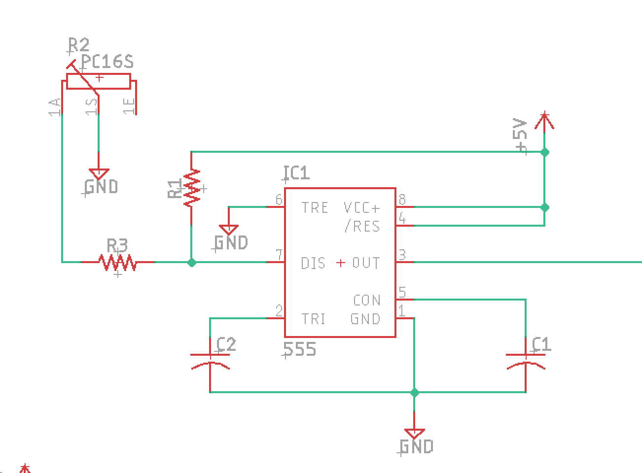
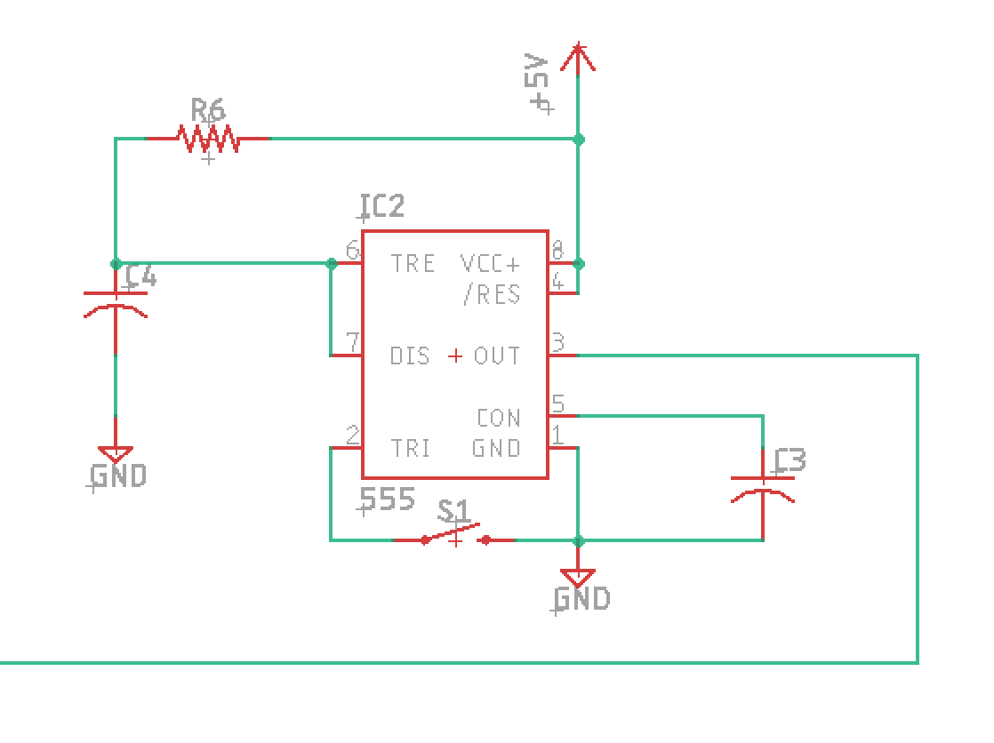
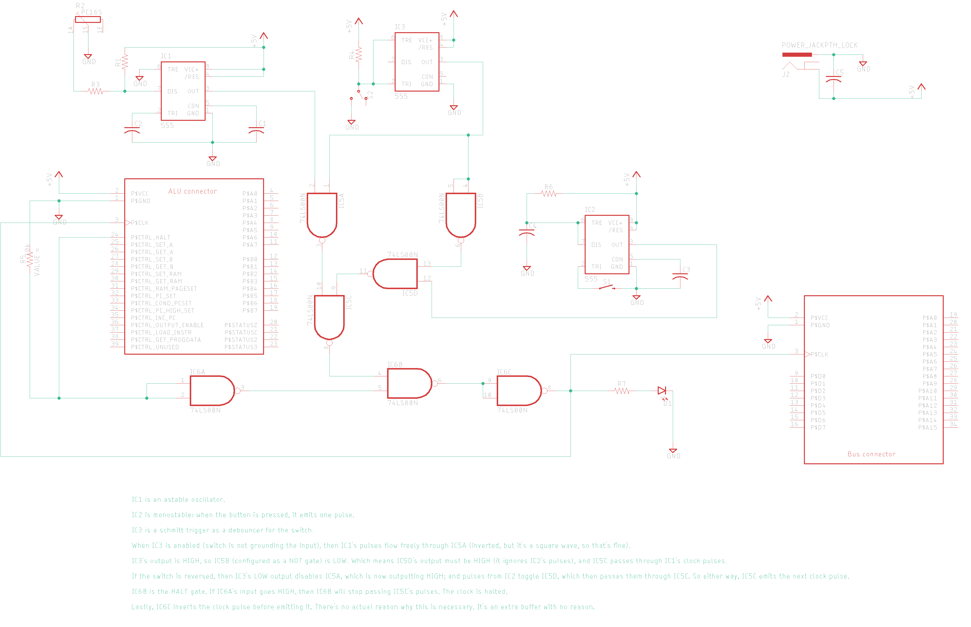
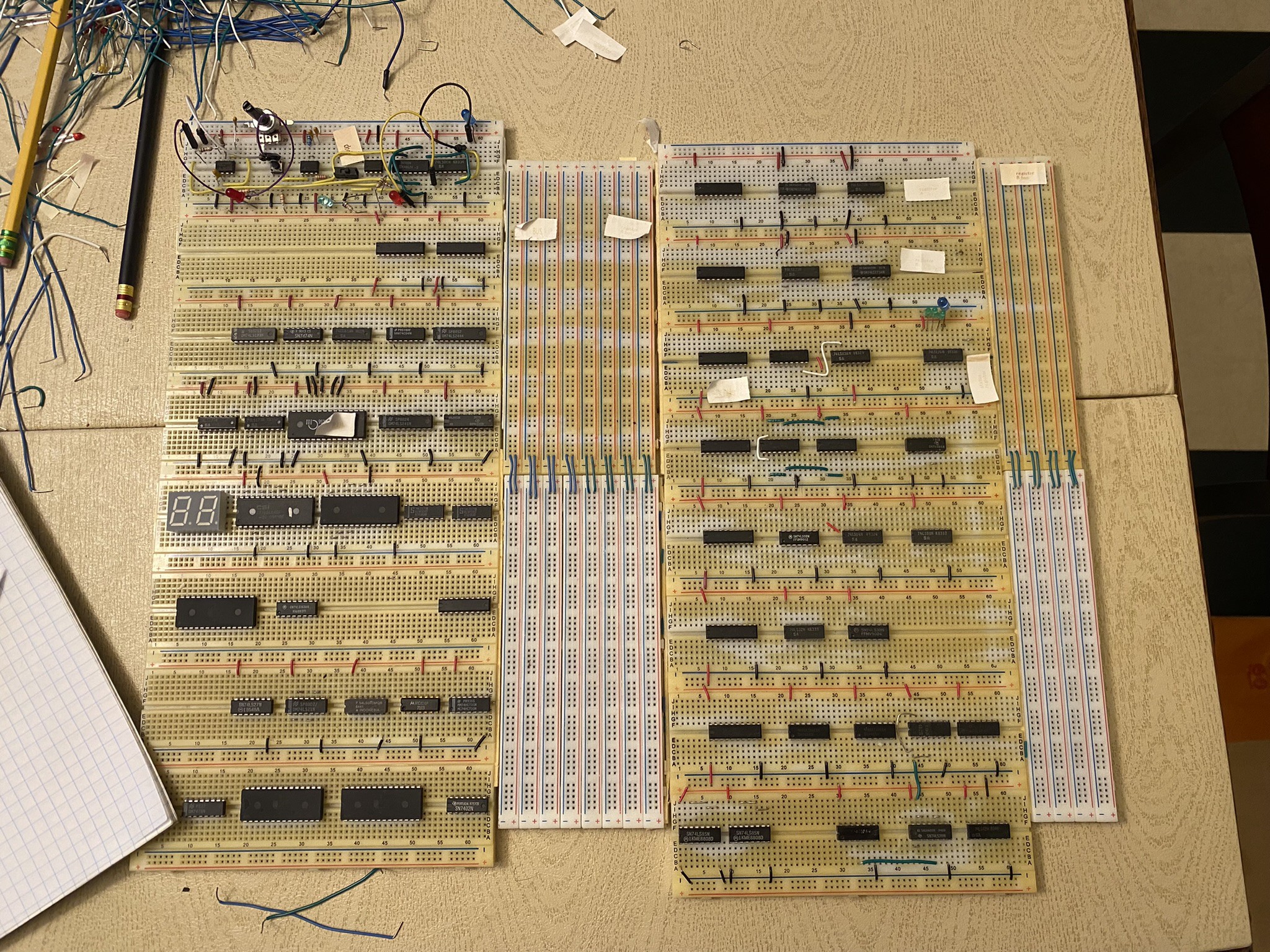
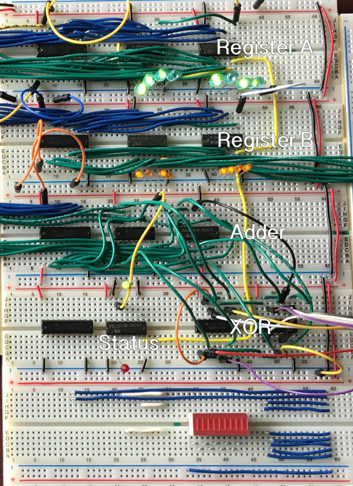
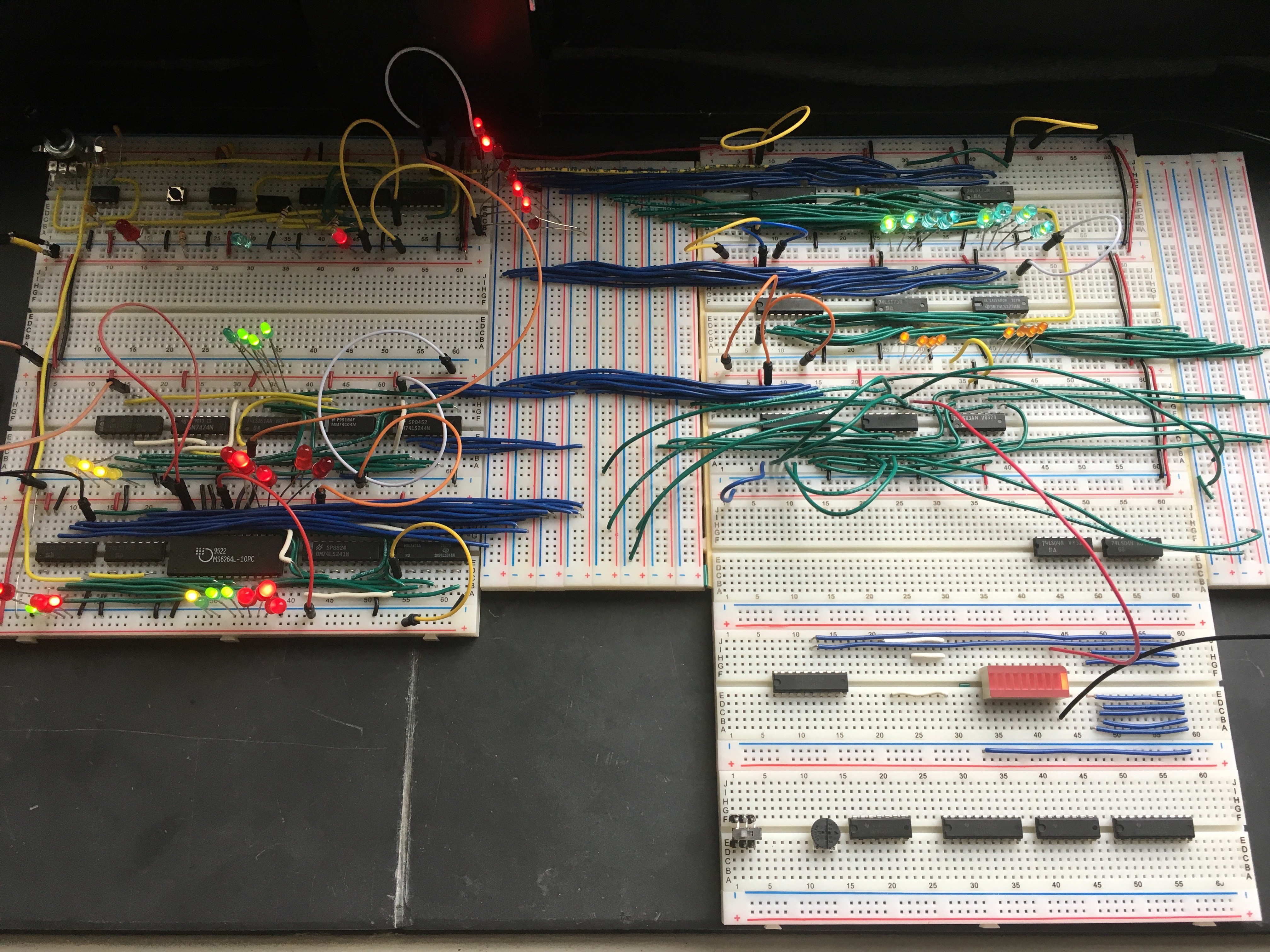
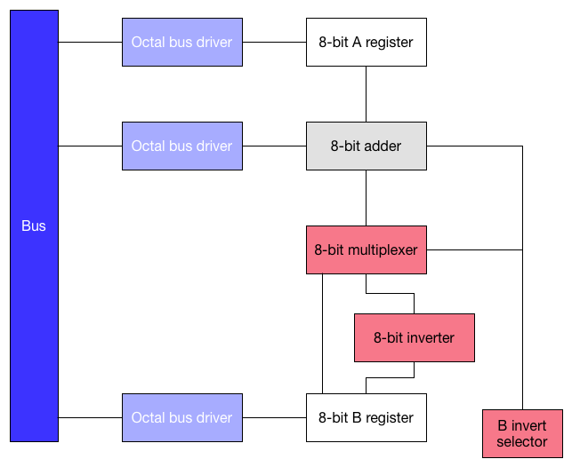
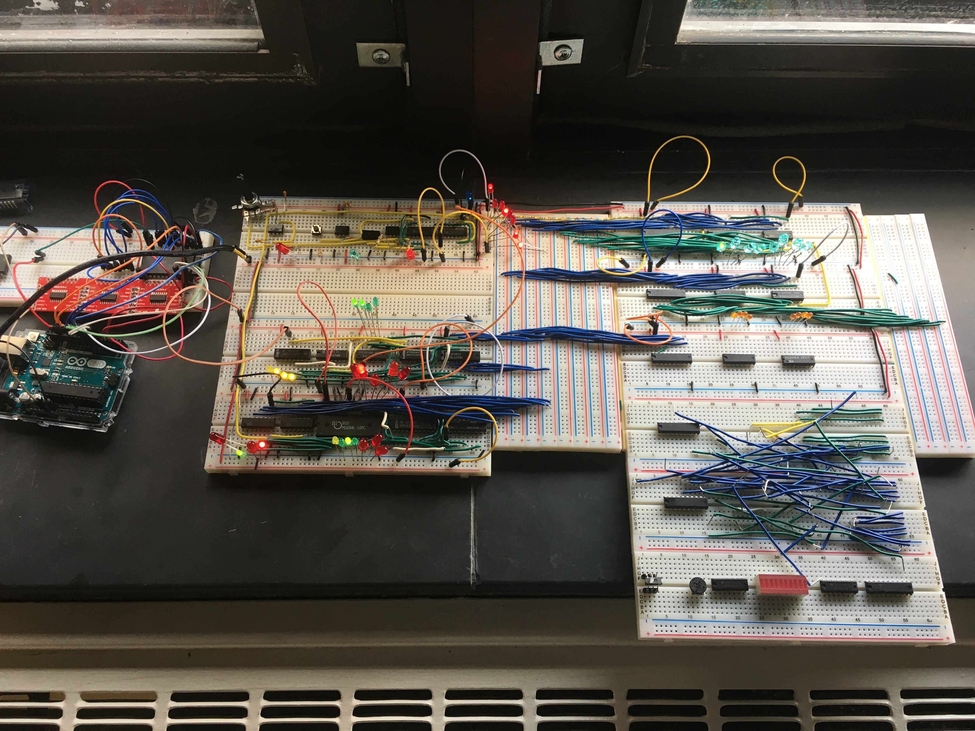
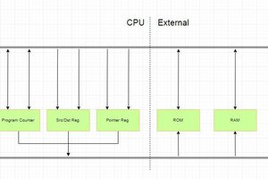
• Redo, Day 1

    Jorj Bauer06/12/2022 at 23:43 0 comments

    Decision the first: yes, I'm going to keep the random-parts-bin-build model. This isn't about making a useful computer; it's about making something useful out of the old parts I've got in the house. So yes, the MC824 with gold leads is going to find a home in this build.

    Which leads to the second decision: the boards will be small, and stacked high. I don't know if I'll build clunkers so I want to be able to experiment and replace easily.

    Third decision: I'm going to use 2x20 pin stackable headers, because they're readily available for the Raspberry Pi. Looking at the signals I've got there are three groups that could be on their own headers:

    1. Core functionality: Power / Ground / clock; 16 bits of address bus (if I actually use it, the design so far hasn't called for one); 8 bits of data bus
    2. Status registers: Power / Ground / clock; 8 bits of register A; 8 bits of register B
    3. ALU / control lines: Power / Ground / clock; 4 bits of status; 16 ALU control lines

    If I were to drop the not-yet-needed address bus that's 47 bits. Since it won't fit on one header there's no reason to drop the idea (yet). But 3 separate headers would be overkill. So I'm going with two: the status registers and ALU will be on one, and the core on the other.

    Given the turnaround time on PCB fabrication I'm hoping to get at least a couple of the boards out at the same time so I can see how they work together (particularly with the stacking bus). And I started in the same place I did with the original -- the clock.

    This clock circuit is built around three different 555 timers, doing three different things. (If I'd had a 556 in my parts bin, it would have been a good choice to reduce the part count. But I didn't, and I have a plethora of mismatched 555s.)

    The first 555 is the heart of the clock. It's a standard astable 555 circuit with a potentiometer to change the frequency.

    But I had two other goals here - a way to stop the clock on demand; and a way to step the clock forward manually. So let's add a switch to stop the clock and something to debounce the switch. The debouncer is another 555, operating as a schmitt trigger:

    And then we've got a button that creates a single clock pulse, using a monostable 555 arrangement:

    All of that's glued together with some NAND logic: if the switch is open, then the astable 555 clock runs free. And if it's closed, then the clock is just pulses from the button.

    One last addition: eventually I want the CPU to be able to HALT itself. So I need a halt control, which will run through another NAND gate at the end.

    The whole thing looks like this:

    Next up is the program counter...

  • "Day 15" or whatever: Rebootski?

    Jorj Bauer06/12/2022 at 01:48 0 comments

    It's been a few ... years ... since I last worked on Detritus. I brought it home after cleaning out my office at work last November, and it definitely didn't survive the trip. So I figure this is a good moment to inventory and document it as-is, and start thinking about the next phase. Building some PCBs that can stand being moved around a little more. (I really don't have space to set this up permanently in my house.)

    I think I've got enough of Detritus built that I should be able to design a modular system that re-implements everything I had on the breadboards. But now I'm asking myself... should I keep the crazy logic decisions I made, or replace them with the "right" chips? Like the AND logic, which ANDs together 4 bits using a quad AND gate... and the other 4 bits using a quad NAND gate and some NOT gates. Do I stay with the chip overkill that came from parts lying around, or do I just buy another AND gate?

    I'm leaning toward keeping the build as-was - continuing on the path of "the right parts are the ones I found in my house" as long as feasible. That was the original goal, after all - use up all the parts.

    The biggest reason I'm questioning that is for problems like the one I mentioned in the last project log -- the program counter not counting well. That's probably related to the mismatched adder chips. If I bake that in to a PCB and it's bad, then I'm stuck waiting for the next PCB before I can fix it. And I've got another piece of detritus sitting around which is an anathema in this project.

    So I've pulled all the wires, and diagrammed as much as I could with what survived the trip. Time to take inventory again, and come up with some sort of modular stackable design...

  • Days 13 & 14: Just Keep Wiring

    Jorj Bauer06/07/2017 at 00:46 0 comments

    ... that's what we do, we wire.

    Wire.

    The OR and XOR were simple and straightforward. AND was a little more complicated, because I only have one quad AND gate; I substituted a quad NAND gate for the other 4 bits and used 4 of the inputs of a 7404 inverter. Another part I'm quickly running out of. I'm starting to think I might have to cross-wire back to the unused inverters in the 7404s lying around the board eventually; each one of these ICs has 6 inverters, and here I am using just a few in each instance.

    Anway: back to the ALU. With the logic gates done, I'm left with the comparator and bit shifters. The comparator is a simple matter of wiring it up per datasheets. A little tedious but not difficult.

    For the bit shifters: my plan is to use two bus drivers like this...

    ... The numbers 0-7 are the bits, 7 being the high bit and 0 being the low. Blue out to the bus, green in from the A register. 'X' are lines held at logical 0 (wired to ground).

    When activated, the left gate winds up shifting 'A' right one bit and putting it back on the bus; while the right one winds up shifting left. (Perhaps I should put them in the other order, so the left one is shifting left. Hmm.)

    But that got me thinking - two ICs to do pretty much the same thing? If I wanted to be clever, I could do this:

    With just this one bus driver, I could rotate right from the bus to the A register (blue to green); or change the direction of the bus driver itself, and I'd rotate left from the A register to the bus (green to blue).

    I never liked rotate instructions, though, and I'm definitely not in this to save on hardware. So I probably won't do that.

    Probably.

    Oh, and I found an error in my program counter! It happily counts in binary: 00000000; 00000001; 00000010; and so on up to 11110000; then 11110001; then 00000010. Or something like that.

    Whoops.

    Going to have to debug that. I've got a '163 counter that I found while re-inventorying my supplies, so I might pull out the '193 and use it in the 8x8 LED matrix display instead.

  • Day 12: A Little Bit of Planning

    Jorj Bauer06/04/2017 at 20:10 0 comments

    I'm starting to find I'm running out of parts! After designing two parts of Detritus to use the exact same chip, which I only had one of, I figured it was time to start laying out everything to figure out what's actually remaining.

    Starting with the ALU, it's straightforward to lay out what I've got. Bus drivers. Mismatched AND and NAND gates with an inverter. OR gates. XOR gates. Comparators.

    And that's where it becomes a little fuzzy.

    I've not thought much about the output display, although I have a couple 7-segment displays, and an 8x8 LED matrix. Driving those is a little more complicated. The program EEPROM; Instruction Register; control circuitry. These need work.

    So, moving on to the displays, then.

    To drive two bytes of 7-segment display, I could take two 4-bit registers; feed each one in to a single EEPROM; and feed the output in to one of the 7-segment displays for each Hex digit. Simple enough.

    For the matrix, though: I want to be able to individually turn on each of 64 LEDs. I suppose that means an EEPROM acting as a logic translator - but it would need to be 16 bits wide, to drive the 8 cathodes and 8 anodes in the matrix. Unless I do something clever.

    I only need to enable one cathode and one anode at a time. Which means I could use 1-of-8 selectors to drive the one, from 3 bits of input each. So with 6 bits of input, we'll get one LED of output.

    But I don't have two 1-of-8 selectors. I've got one. And a 1-of-10. That'll do.

    The selectors invert the output, which is great for the anode side of the LEDs. For the cathode I'll need +5v out, which means 8 inverters. I've got some 7405 hex inverters I can use. And that's enough for turning 6 bits of input in to one LED of output - but I still need to get those 6 bits of data.

    Well, if I take the 8 bits of data being input; 3 bits of "which row is this"; and 3 bits of "which LED in that row is the one I'm currently trying to light up" - then we can take a total of 8 bytes of input and turn them in to each of the 64 bits of output individually, in sequence.

    That all means a 555 timer that's feeding an adder which resets at 64 (counting from 0 to 63); some sort of RAM to hold the 8 bytes of data; and a way to program it from the bus. Well, that last bit is a little difficult; if the data from this RAM is tied to the EEPROM and a timer/counter, then I'll need some complicated logic to decouple it when the RAM needs to be updated with new values.

    Unless.

    There's a type of RAM that's designed just for this - dual-port RAM. A dual-port RAM has two distinct busses - and either side can read or write at will, independently. I only need 8 bytes, a very modest dual-port RAM. Perhaps I can find one on eBay cheaply.

    If this is how it plays out, then the design looks something like this:

    Time for some parts shopping, then. I need a larger EEPROM. I've already run out of latches. And I need a dual-port RAM.

    Perhaps the whole thing winds up looking like this, then...

    ... lots to do there!

  • Days 10 & 11: I've Got the Power

    Jorj Bauer05/31/2017 at 23:53 0 comments

    Day 10 started with a simple "clean up the wiring" - and quickly went downhill. Something wasn't right; I was seeing odd results from the adder. Inconsistently. Often while running off of the main clock. Not very often when running by hand.

    So I went debugging.

    The obvious culprit would be power drop around the board. Quickly, then: drag out the multimeter! Voltage near the point where it connects to the board? 4.9 volts. What about over at the adder? 3.2 volts.

    Yeah, I'd say that's the problem.

    These solderless breadboards have pretty significant internal resistance. Which means the power connections that are jumping board-to-board-to-board are a problem.

    So these two days are entirely: trace some wiring; remove some wiring; replace the wiring; trace more wiring; remove more wiring; get fed up and rip out some wiring that was probably fine; solder in new wiring; rewire with temporary wiring and test; rewire with more permanent wiring.


    Next up is some very boring wiring for the remainder of the ALU (and you thought all the wiring I just did was boring? Hah!) - invert, AND, OR, XOR, and compare.

    The B register inverter is already part of the adder (for "subtract twos compliment"), so that will probably be next; it just needs to be wired to the bus. Which needs to be physically longer to accommodate all of these modules:

    I've also been thinking a little about output. I might like to hook up some 7-segment displays. I have a mess of fairly boring 7-segment drivers that just decode the numbers 0 through 9; I'd prefer hex, though. So maybe the Intersil 7218, a fancy 7-segment driver? It has a hex mode, and I've got three of them. Well, one Intersil and two MAX 7218s. The Maxim version is slightly more fancy with an "update just one digit" mode that the Intersil didn't have. I probably won't take advantage of it; I probably won't even take advantage of the 7218's ability to drive 8 separate digits. Two digits is sufficient to display what's on the bus, which makes these officially overkill.

    And yet, this also seems insufficient in terms of final display. I'm not sure what I want this computer to be able to do, but I suspect it will involve ... Pong. Which would mean some better form of display, maybe? Hmm. I have a bunch of shift registers, and some LED matrix modules...

  • Day 9: Status Register and Subtraction

    Jorj Bauer05/24/2017 at 10:21 0 comments

    Remember all that hoo-ha over the subtractor yesterday? The insane architecture where this seems to be the way I'm going to multiplex the input in to the adder, so that I can perform twos-compliment math for subtraction?

    Well, funny story.

    I placed orders in three different places for the parts for this build. Looking at them last night, I realized that I'd accidentally ordered two XOR gates ... from two different vendors.

    That's right, one of the packages that's still enroute has something like $1 in parts that will turn that multiplexer design in to a single box in this architecture:

    Harrumph. I feel like my hard work was wasted, and now I'm not gonna get to use the kooky logic I built. Like running a copy of VMWare on Windows, which is running on a qemu emulator on a Linux machine. Totally impractical but there's some sense of accomplishment in there. For whatever reason.

    So this is the result at the end of today's lunch:

    ... there was to be a time lapse of the work itself, but apparently I shut off the camera right after it started. Well, maybe tomorrow.

    The changes today: the wiring to the adder was cleaned up; then I added the beginnings of the status register, and wired in the XOR gate for the input from the B register to the adder.

    I realized two things in the building stage. One: I wanted an INVERT operation in the ALU, so I might as well use the 8-bit XOR for that. Slap on a bus driver and it's a done deal. And Two: I need to put in a status register for the Carry flag.

    I'm not entirely sure that I need to put the status register on the bus yet. I'd like to limit the status register to 4 bits, because I have only one '173 remaining. And it has a built-in TRIS, so maybe I don't need a bus driver for it... I suppose that all depends on whether the control logic needs the carry flag at the moment it has been asserted from the ALU, or during a subsequent operation. We'll see.

    Here's the ALU from the photo above, with some annotations:

    (The wiring from the XOR to the adder obviously needs some cleanup tomorrow.)

    The status register, with its lonesome one bit, is showing that A (%1110 1011) + B (%1010 1101) has carry set (the LED above the status register); but that last clock cycle, it was not set (the LED below the status register). When the clock next pulses, the status register will latch in the carry.

    Maybe that means that the ADD microcode will need an extra clock cycle to be sure that the carry flag is appropriately set. Thinking about it, that seems fine - I've allotted two microcode clock cycles for each machine instruction - and for the ALU operations, I don't have anything in the second cycle yet. I'll note this for later, I think, and we'll see how the control logic fits when we get that far.

    Goals for Day 10:

    • move the status register; I think it's in the way
    • clean up the XOR wiring
    • put XOR on the bus
    • build AND and put it on the bus

    ... but I'm quickly running out of board space. I need to order some more solderless breadboards so I can extend the busses. And I'm almost out of blue wire, which I'm using for all of the bus interconnects. More of that should be arriving today; I might have to put off some of the bus connections another day.

  • Day 8b: ALU adder

    Jorj Bauer05/23/2017 at 00:33 0 comments

    Should be simple, I thought! Just a little baby step: hook the A and B register inputs in to the two 4-bit adders. Leave the complicated stuff for another lunch.

    So: bus A to the adders' A inputs. Bus B to the adders B inputs. The Octal bus driver (one of the '245s I bought) is already connected to the bus; just need to wire up the Σ outputs to the '245. Aaand... nothing. Nothing? And why is one of the bits in register A suddenly being pulled to ground when I wire up this unrelated B register input to the other adder? Oh, and look! It's getting pretty hot...

    Yank power. Quickly.

    Oh, right. The adder on the left is a 74LS283, which I just bought because I only had one adder. The one that I had is a 74LS83. Which is an entirely different beast, with a different pinout.

    Fortunately for me, I didn't destroy it by running power and ground to the wrong pins. And then I also didn't destroy it by tying ground to +5v and Vcc to GND, because the ground pin is on the north side of the IC and Vcc is on the south side, the opposite of normal these days.

    Only took me about a half hour to diagnose what the heck I wired wrong and re-wire it badly. I guess lunch tomorrow is going to involve some clean-up of those higgledy-piggledy green jumpers.

    The math even checks out! Whoohoo!


  • Day 8a: convoluted ALU design

    Jorj Bauer05/22/2017 at 09:24 2 comments

    Having picked a crazy overkill instruction set, it's easy to see how those functions map out in an ALU. 2 registers; an adder; and four logic functions. I spent some time over the weekend thinking about how this maps out to a final design, and in particular realized that I've run a little short on a particularly important IC.

    So, thinking a little about the adder, which should be fairly straightforward...

    ... where that XOR is the selector of whether we want to input B, or an inverted /B, so that we can subtract instead of adding.

    But I only have two quad XOR gates - both of which I just bought, because I didn't have any in my original stock - which means I can either use them for the adder's "invert" operation selector; or I can use them for the XOR function itself.

    Hmm.

    If the ALU's XOR operation is supposed to be the A register XOR the B register, then there's no simple way to re-use those two ICs for both purposes. I could stick two octal bus drivers around it, selecting an output path to either the adder or the bus; and an input path either from the B invert selector or the A register.

    That doesn't feel like what I want, though. This is using a bunch of bus drivers for selection; it doesn't pay any particular attention to what other ICs I have lying around. Looking for another solution with the parts at hand, then... what if I use some of the multiplexers I've got to select either B or an inverted B as an input for the adder?

    Ooh. That looks much sexier. A couple 7404 inverters to construct /B, and some multiplexers to select one or the other! I like it. But the devil's in the details: I have a rather motley assortment of ICs and I don't know that I have what I need. Or, rather, I know I don't have enough of any one part to satisfy that demand.

    For starters: I have two 74LS153s. They work like this:

    It's designed to pick one of the 4 bits of data input, in two places. I can use it like this, to select 2 bits from either B or the inverted B input:

    And you probably now see just the level of crazy I'm going to with this plan. Since I have only two of these, I'll get just 4 of my needed 8 bits of virtual switch. Hmm. Well, I've got two 74LS151s, which are similar 1-of-8 multiplexers:

    Well, I could use each of those for 1 more bit. Which gives me a total of 6 bits. Still not enough.

    I've also got some 74LS139s, which are 1-of-4 decoders. A decoder is basically a multiplexer where the inputs are all logically tied high. The '139 inverts the output bits, which means it looks like this:

    Hmm. If we add a NAND gate to the two middle bits of that output, then this looks like XOR. Which means that we can take one bit of B, and the B-Invert selector, we get two bits out which are either B or /B:

    I feel like I just struck gold. I wish I had enough of those to build the whole 8 bits; this has a certain kind of sexiness to it.

    But I don't have enough of any of those, so I'll have to mix-and-match.

    I suppose I should try to minimize the board space used? I mean, I've already thrown in the crazy towel, so there's no sense trying to optimize for power draw, or number of ICs. Yes, yes, I'm looking for an optimization in some way other than "just buy two more 50-cent quad XOR ICs." I'll pretend you didn't even think that.

    Since the 74LS151s would be mostly dead space - yielding just 1 bit of output each - I think I'd rather not use them. Which would mean using 2x 74LS153s; 1x hex inverter (using 4 bits to drive the '153s, leaving two inverters unused); 2x 74LS139; and 1x quad NAND gate.

    There's one final bit of insanity thrown in there. I'm running out of 7404 hex inverters... but I have five 7405 open-collector hex inverters. Which, if you add a pull-up resistor to the output, are basically the same thing.

    Well, I guess this will be interesting to implement. I'm sure the wiring will be a nightmare, and if there are any problems with it, debugging will not be a barrel of monkeys. But it satisfies my design goal! Look at all those ridiculous ICs I'll finally be...

    Read more »

  • Day 7: Rebuilding Registers

    Jorj Bauer05/20/2017 at 12:36 0 comments

    Since I've given up on my X and Y registers, it's time to pull them out and rewire them as A and B registers in the ALU.

    Since the ALU will heavily wire these two registers, I've decided to add two more 8-bit busses vertically alongside the ALU. The A bus will be on its left; the B bus on its right.

    My '245 transceivers have also arrived in the mail. The X and Y registers didn't need bus transceivers; the registers are already tri-stated, which made that easy. But with the A and B registers, I need to be able to hard wire them to the adder, in addition to selecting whether or not they go out to the bus. The adder itself will be outputting to the bus, in addition to the A and B registers both being enabled for output to the ALU simultaneously; all three can't write to the bus. So I'm going to need separate bus transceivers for A and B.

    As painful as it is to rip apart what I've already wired up, here it is in a better form...

    You can see the space on the left that used to *sniff* hold the X and Y registers. They're now the top of the ALU board on the right.

    I've started positioning ICs for the rest of the ALU, but none of it is wired.

    So, maybe it's time for a little video!

    I've tied the program counter increment line to the clock; enabled the PC output to the bus; and enabled the inputs from the bus for the A and B register as well as the RAM memory address register. Lots of gerblinkin lights, mostly showing the current PC, delayed by one clock cycle.

    The lights that *aren't* showing the program counter: three LEDs on the clock in the upper left, and the eight red LEDs around the RAM on the lower left. Those red LEDs are showing the (random) contents of RAM at each address as the memory address register is updated.

    Next up will be the adder. Hoo boy, I've got a doozie hiding in there...

  • Day 6: designing the instruction set

    Jorj Bauer05/20/2017 at 12:14 0 comments

    First of all: in thinking about the ALU and the parts I've got, I would have to order more register latches if I want to keep the X/Y register along with at least one register for the ALU. So I'm going to scrap that plan; I'll have two registers that are tied to the ALU, and I'll make them both general purpose.

    Now, with A and B ALU registers, what functions do I want the ALU to perform?

    Certainly, ADD and SUB. I've got enough gates for AND and OR, and I just placed an order for XOR. I'd like INVERT. And bit shifts, left and right (LSL and LSR).

    Each of those will need an output control gate to the bus, or a wicked mess of multiplexers that select which goes to the bus. I'll stick with individual outputs, which means they'll need individual control lines.

    Exactly what control lines do I have (and think I'm going to add)? Well, maybe these 15:

    0Clock Halt
    1A register input from bus
    2A register output to bus
    3B register input from bus
    4B register output to bus
    5RAM in
    6RAM out
    7RAM memory register set
    8PC counter set
    9Conditional PC counter set
    10PC high bits set
    11increment PC
    12Output Enable (bus => output system)
    13Load instruction register
    14Program data byte => bus

    If I add the 9 ALU actions, then that's more than 16 bits of control. I'd really rather not have *three* EEPROMs running the control logic. And if we just add one more control line - an ALU Active line - then maybe we can encode the specifics of *which* ALU action in the opcode itself.

    Which begs the question: what are the opcodes? Do we have enough bits to be able to do that? Hmm...

    0x00NOPNo-op.
    0x10 <byte>LDA #immediateLoad a value in to A
    0x20 <addr>LDA $addressLoad A from memory address
    0x30 <byte>LDB #immediateLoad a value in to B
    0x40 <addr>LDB $addressLoad B from memory address
    0x50 <addr>STA $addressStore A in memory address
    0x60 <addr>STB $addressStore B in memory address
    0x70 <page>MEMPAGE $pageSelect RAM page $page (4 or 5 bits?)
    0x80ADDADD A + B => bus
    0x81SUBSUB A - B => bus
    0x82ANDAND A and B => bus
    0x84OROR A or B => bus
    0x86XORXOR A xor B => bus
    0x88CMPcompare A and B; set Carry status flag?
    0x8BINVInvert B => Bus
    0x8CLSLShift A left 1 bit => Bus
    0x8ELSRShift A right 1 bit => Bus
    0x90JMPJump to new program counter address
    0xA0JCSIf the status Carry flag is set, then jump to program counter address
    0xB0HALTHalt instruction

    That looks plausible. The high 4 bits of each instruction will feed the address input of the control EEPROMs; the 8 bits of output from those EEPROMs will feed the 16 control lines through the computer.

    The low 4 bits of the instruction will be tied to logic that selects ALU functions. It's tempting to run them through another EEPROM, but then I'm back to three EEPROMs running the control circuitry. Instead, I've got some 1-of-8 decoder ICs (like the 74LS138) which I can use. So three of the low 4 bits will feed a '151 or similar; while the fourth low bit will enable the "invert B" input in to the adder, for subtraction.

    Nice, this might even work.