 Krinkleneck
I thought this log would have come a few hours earlier, but it didn't work out that way. I am ordering parts to do a test build of the power system. I am only doing a segment of the build to see that I get appropriate voltages out of one lane of the charging system. I am doing this because a couple of the components that I am looking at don't specify some of the details that I need, and I will need to shotgun/plug and play a couple capacitors to get it right. I am not satisfied with the component cost that I have achieved. So I will be most likely replacing a couple components. I have put out a partial schematic for what the power delivery from the battery should look like. The components with blanks are the in question components. This is because while I'm fairly sure that I will be using the components I have listed before I have an inkling feeling there is failure afoot in this design. So I have left some key components blank. There are also some discrepancies. When the power leaves the boost converters they will all merge and get divided up in parallel to each regulator. Then each of the three regulators will supply 2 peripheral ports. This should help not only conserve probability of overload due to any follies that I make when I am making peripherals.
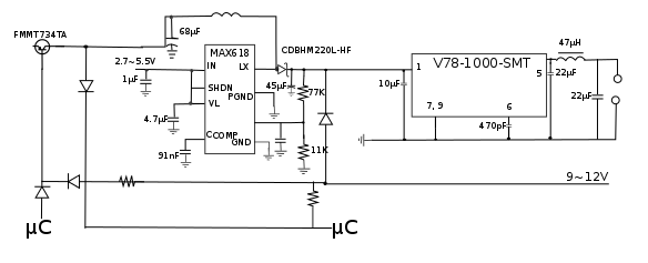
Now this isn't the full design, but instead it is a partial test design. I need to test out how I am going to be dealing with the step up. Normally I would just just boost convert a low DC source to the voltage that I need, but I need to subdivide and regulate the current. Each 2 peripherals share the maximum current of 1 amp. Since most regulators I have seen require at least 1.5v because of drop off voltage I had to overshoot. If I am overshooting I might as well try to keep the line saturated. I will fine tune it into the USB voltage range.
Now how I am controlling when the battery is charging or discharging is through both digital logic and analog control. The charger is attached in a way that it turns off the flow of DC through the battery circuit and assumes control of the circuit or upon the command of the μC. Since I have opted to have all devices attach to the battery circuitry before being a power user I went with a Darlington PNP transistor. Once the device has confirmed through I2C, or another preferred protocol, the μC will disable the PNP and activate an NPN or a FET and receive the power as a normal device user should. This also leaves the option to completely isolate most of the power using components by telling the μC to disable the power out and not the power in. This would be an excellent use for sensitive projects that can't be directly in contact with the Mainboard. It also allows a user to have a controlled power down sequence. That way when the power gets low the user can decide which ports get shut down first. Or they can use it in any way that they can see manipulating the power.
Discussions
Become a Hackaday.io Member
Create an account to leave a comment. Already have an account? Log In.