Click here to access the official unit website.
Table of Contents:
1. Fundamentals of High Speed Digital and Mixed Signal Circuits
2. High Speed Digital Circuits
3. High Speed Digital Design - Case Study
5. Mixed Signal Circuits
6. Mixed Signal Design - Case Study
7. MSD Design Review

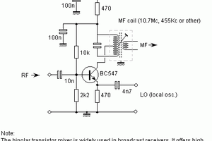
 agp.cooper
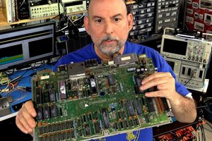
 Bil Herd