There is a major limitation with circuit schematics: 3 circuits (with the same schematics) may have significant performance differences which are a result of the physical layout of the circuits. Therefore it can be said that how a circuit is implemented is what matters. Alternative implementations exists for any schematic therefore some important aspects of most designs are not well described by schematics.
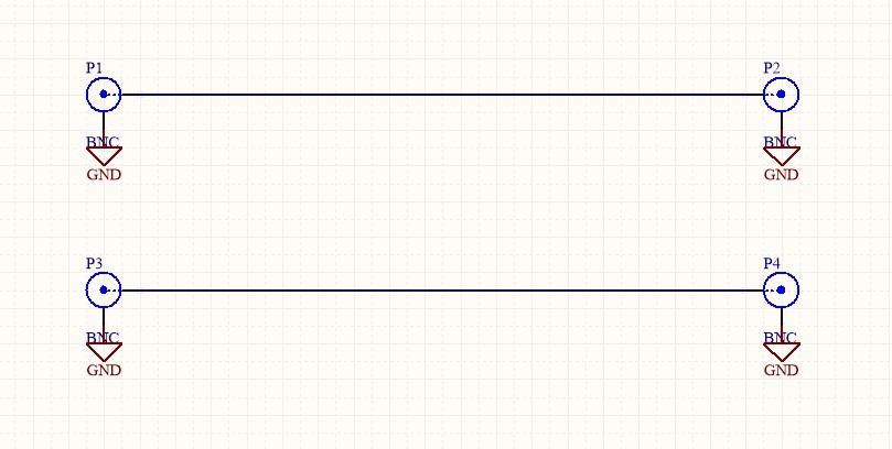
The circuit schematic above shows two adjacent traces that are connected to BNC connectors.
Although they are not physically connected; each wire linked by mutual inductance and mutual capacitance. Mutual quantities can couple circuits that are not intentionally linked, causing crosstalk.
Each pair are connected by series resistance and inductance, having capacitance to ground.
These unintentional resistance, inductance and capacitance values are referred as parasitics.
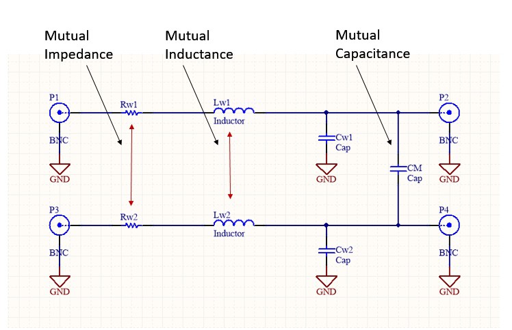
It should be noted that Rw1, Rw2, Lw1, Lw2, Cw1, and Cw2 are not actual components and they are representing the unintentional parasitic behavior of the two wires. In the circuit schematics the mutual reactance components were all zero since they are not physical components. Therefore schematics are said to be limited in terms of displayed information and may be misleading.
The mutual reactance between two wires are determined by the layout of the circuit, for example:
- Wider traces reduce the mutual impedance
- Proximity to GND layer increases the mutual capacitance
- Increasing the separation between the two circuits evidently reduces the mutual inductance and capacitance.
In the context of PCB design the concept of return current paths are often misunderstood. Current flows in loops, e.g. a signal current that flows along a trace has a corresponding returning current which should be handled carefully since it plays a huge role in circuit performance.
Signal Integrity and Crosstalk
Signal integrity describes the properties of a signal arriving at its intended receiver. The signal may be degraded by poor design of the signal path or by poor termination.
Crosstalk is the unwanted coupling of two or more circuits. In other words, crosstalk describes the contamination of the signal on a victim circuit by a signal on a different aggressor circuit. By nature analogue circuits are typical victim circuits whereas digital circuits are typical aggressor circuits. More details about this will be provided under the title "Mixed Signal Design" where both digital and analogue signals are accommodated on the same PCB. Poor circuit layout increases the crosstalk!
DC & Low-frequency Signals:
The returning current takes the path of the least resistance (in fact it is the path with the least impedance but they are the same for low frequency circuits).
High Frequency Signals:
The returning current flows under its signal trace. For H.F. the path of the least impedance is the path of the least inductance which is right under the signal trace. As a result the return paths are self-managed by inductance given that an uninterrupted SGND plane adjacent to the signal plane is provided.
Advantages of SGND Plane are as follows:
- Return current can flow directly under its signal trace.
- The loop area is minimized and hence E and H fields are localized.
- Signal integrity is improved and the crosstalk is minimized.
The following coupling mechanisms are responsible for crosstallk:
1. Mutual Capacitance:
The figure below shows the lumped component view of mutual capacitance.
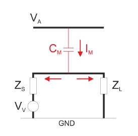
Every unideal resistor has a small ( < 1pF ) shunt capacitance in parallel with its ideal resistance. Capacitors store energy in their electric (E) field. Likewise all conductors with different potentials store energy in the E field created between them. Interaction of E fields create mutual capacitance. If the E field of the aggressor is sufficiently localized there is no crosstalk due to mutual capacitance.
Mutual capacitance depends on layout: the E fields can be localized by providing a nearby returning path (ideally a SGND plane) to the signal trace.
2. Mutual Inductance:
The figure below shows the lumped component view of mutual inductance.
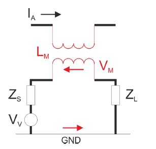
Every unideal resistor has a small ( < 1nH ) inductance in series with its ideal resistance. Inductors store energy in their magnetic (H) fields. Likewise, and current carrying conductor stores energy in their magnetic field. Interaction of H fields create mutual inductance. If the H field of the aggressor is sufficiently localized there is no crosstalk due to mutual inductance.
Mutual inductance depends on layout: the E fields can be localized by providing a nearby returning path (ideally a SGND plane) to the signal trace.
Relative importance of mutual capacitance and mutual inductance:
Now the question is which one is more dangerous?
Modern high speed digital circuits operate at low impedance (high rate of change of current) and low voltages (low rate of change of voltage) as a result, mutual inductance is a greater problem.
3. Antenna Effect:
It is possible to create an antenna effect by poor circuit layout - although it is unlikely to be made by mistake.
4. Shared Impedance:
GND plane with non-zero impedance is the source of the shared impedance.
If the return currents of one or more circuits are sharing the same return path and if the the ground has non-zero impedance certain amount of voltage drops across this impedance.
The formed potential difference by one circuit is treated as ground by the other circuits.
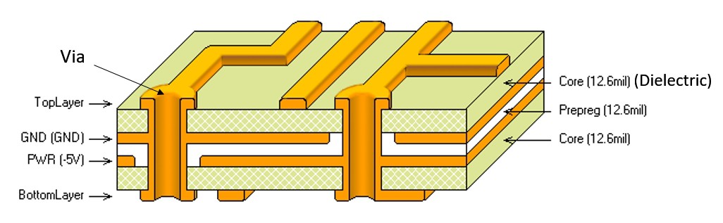
Figure above shows an example PCB layer stack where the top and bottom layers are signal layers and the enclosed two planes are for power and ground.
The Net Inductance of a Trace
- Wider traces reduce the inductance of the trace
- Traces that are closer to their return plane (achieved by a thinner dielectric layer) lowers the net inductance of the trace
Net Inductance of a Plane
- Thinner dielectric layer also reduces the net inductance of a plane
Lower net inductance evidently reduces the mutual inductance and hence the crosstalk due to mutual inductance.
Via placement is very important in minimizing the net inductance, i.e. the performance can be improved with no additional costs. On the other hand, misuse of vias may cause impedance discontinuity and degrade the signal.
Discussions
Become a Hackaday.io Member
Create an account to leave a comment. Already have an account? Log In.