 polyfractal
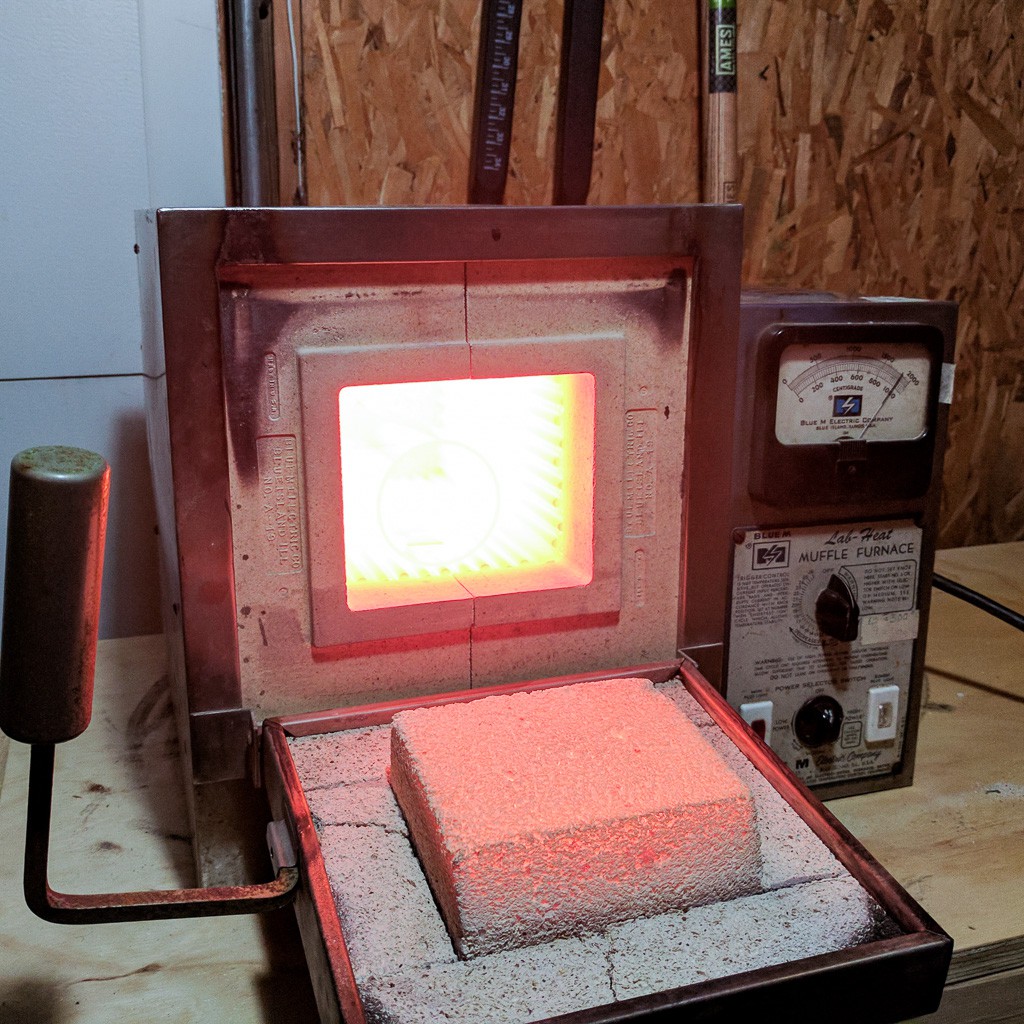
The best part about projects like this is getting to scrounge up new-to-you toys to play with. In this case, I get to play with a 1000C bench furnace. I mean, just look at that baby glowing. Fun!
So while I sort out the details of The Plan, I figure I can start practicing some of the logistical parts of IC fab. The first step of an NMOS process is growing a thick layer of silicon dioxide. This is known as the field oxide and serves to isolate transistors and other components from each other.
 Because its job is to simply isolate components, it's grown relatively thick. The goal is around 5000 angstroms (500nm). This is accomplished at high temperatures.
But first, we need to clean the wafers. There are a number of cleaning options used in wafer processing.
- AMI clean: acetone, methanol, isopropanol. A relatively gentle clean that uses consecutive solvents to remove organic particles (and the "scum" from the previous solvent)
- Piranaha solution: three parts H2SO4 to one part 30% H2O2. An extremely aggressive acidic solution that etches away the surface of the wafer, taking organic matter with it. Exothermic and rather unpleasant to work with.
- SC-1: four parts purified water, one part 30% H2O2, one part NH4OH. A basic solution used to remove organic matter. It works by rapidly oxidizing the wafer surface, then dissolving the oxide layer. Organic particles are trapped "lifted off" during the dissolution of the oxide. The standard recipe is 4:1:1, but research shows higher dilutions are as effective (e.g. 40:1:1)
- SC-2: five parts dH2O, one part 30% H2O2, one part HCl. An acidic solution used to remove metal contaminants. Works similar to SC-1 by oxidizing + dissolving, but attacks metals that were left by the other cleans
- Plasma cleaning: Plasma is an effective method of cleaning multiple contaminants. The soup of ions and electrons in plasma react with surface contaminants and help break them up and lift off the surface. High velocity particles impinge on the surface and physically dislodge contaminants.
The cleaning method is chosen largely based on the quantity and nature of contamination, and compatibility with other steps. I don't have any sulphuric acid on hand (yet), and also don't particularly feel like working with boiling hot, oxidizing acid.
So I settled for a gentler clean. I did an "AI" clean (acetone + isopropyl) clean to remove bulk organic residue, then a dilute RCA clean (SC-1 + SC-2) to remove some more gunk. The literature says a dilute RCA works well, which is convenient because I also don't have concentrated hydrogen peroxide (yet).
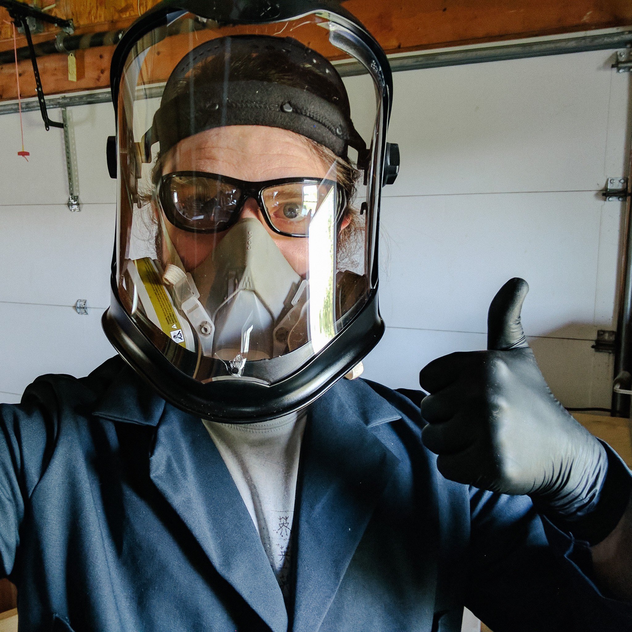
Remember kids, always wear your personal protection gear! For me that means respirator (rated for solvents, ammonia, acid and base fumes) safety glasses, face mask, nitrile gloves and lab coat. I also have thick neoprene gloves on hand to work with nastier mixtures.
All of this was done on a glass bench (easy to clean) and with plenty of ventilation, fire extinguisher standing by. Safety first!
After the cleaning procedure is done, it's time to start growing some oxide. Silicon Dioxide can be grown either "wet" or "dry", both at very high temperatures (1000+ C). Wet oxidation uses water molecules to accelerate oxide growth, allowing thick layers to form very quickly. The oxide that's grown is somewhat porus due to it's speed of development.
Dry oxidation is done in a dry (surprise!) atmosphere, often an oxygen rich mixture with a bit of HCl to help capture metal ions. Dry oxidation makes a much nicer oxide layer, but is also a lot slower.
Field oxides are traditionally done "wet" due to their thickness. A 500nm oxide takes ~1.5hrs in a 1000C furnace. Dry takes something like 40 hours.
I loaded my muffle furnace with a quartz tube to help shield the wafers from contamination, then I placed the cleaned wafer chips inside and cranked up the heat. Ideally, you'd only add the wafers after the furnace is up to temperature... but my furnace is old and takes a long time to heat up, and it's not very fun to load samples into a 1000C furnace.
So I just loaded them from the beginning and tried to adjust my math a bit. I squirted water into the furnace (very scientific and repeatable, I know) at semi-regular intervals to keep the air humid.
The furnace really is quite an impressive sight at 1000C. You can feel the heat through thick leather welding gloves in just a few seconds... I need to get some proximity gloves I think.
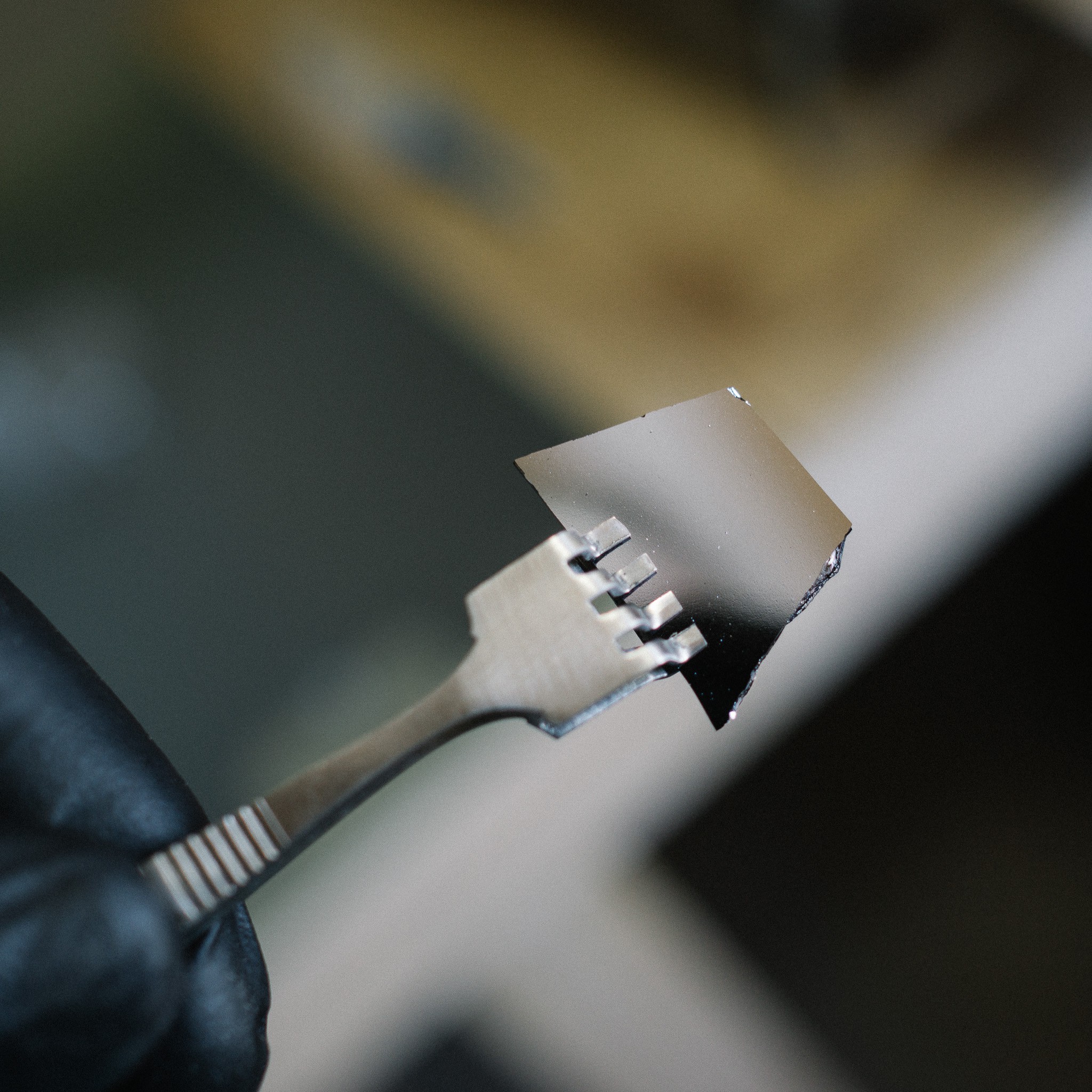
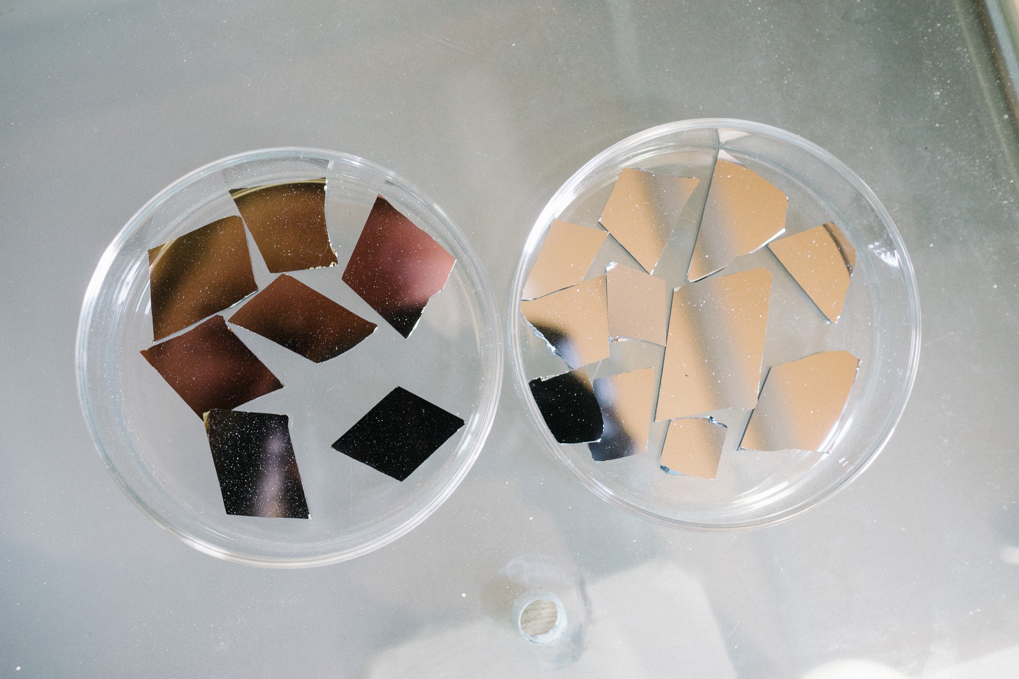
After the bake, I cooled the furnace and checked out the wafer chips. Here's what a pre-oxidized wafer looks like:
And here is an oxidized sample:
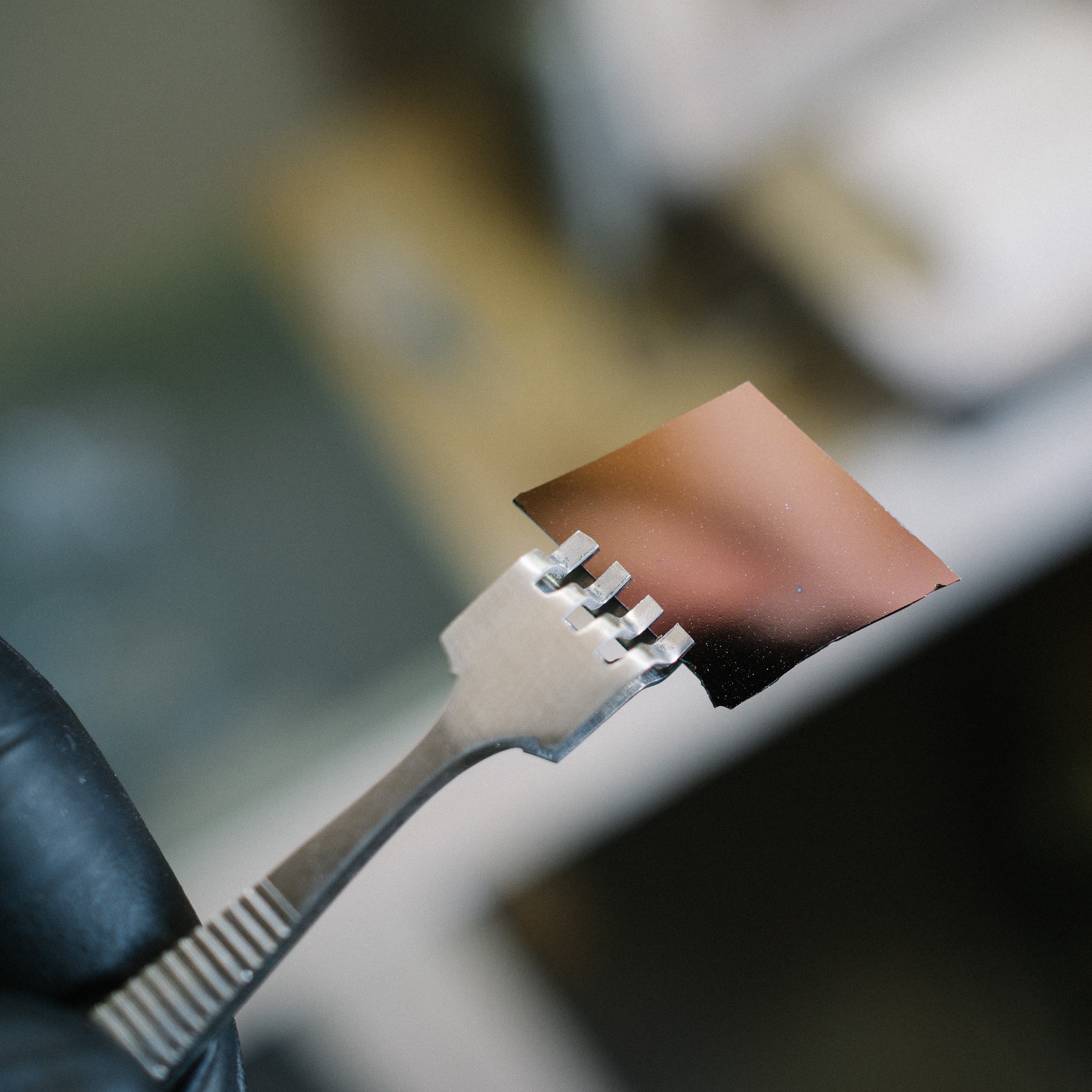
Notice how the wafer is more of a red/orange? That's the oxide. Well, not really. Silicon Dioxide is transparent. But some light reflects off the top surface of the oxide, while some light passes through and reflects off the underlying silicon, which then travels back through the oxide and interferes with the first reflection.
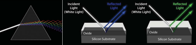
This interference forms a color, and the exact color depends on how thick the oxide is. Which provides a handy way to estimate the thickness of your grown oxide. There are charts available which show expected color-by-thickness.

If I had to guess, I think I overshot my 500nm target. I think I probably landed around the 650-700nm range, due to the slightly orange-red cast. I don't think it's one of the lower orders due to how long it was in the furnace. Hard to say though, since color changes depending on viewing angle (you're supposed to view it perpendicularly but it can be challenging with light sources)
There's also a load of particulate contaminant on the wafers, which is almost certainly silica dust from the refractory brick. I was hoping the quartz tube would shield the wafers from the worst, but apparently there is more convection (and particle shedding) than I had expected. I'll have to see about "plugging" the ends of the tube.
All in all though, I'm pretty pleased.
Discussions
Become a Hackaday.io Member
Create an account to leave a comment. Already have an account? Log In.
Dude, you are epic :-D
Its rare I dont have words, but this is one of those occasions. I got a bit of venturi envy the other day when you posted about the oven, but this?? I am officially jealous XD
Are you sure? yes | no
Thanks! I was pleasantly surprised how well it worked :)
Are you sure? yes | no
Hmm, fun thing to have a hand stuck in. Exciting!
Are you sure? yes | no
Hehe...I took a bit too long moving things around once and realized the outside of my (thick) leather welding gloves were starting to smoke. It really doesn't mess around!
Are you sure? yes | no