Close
0%
0%

YGRECmos

The YGREC architecture, this time implemented in CMOS

Similar projects worth following
This is a crossover between the other YGREC projects, that use discrete transistors or relays, and the "Discrete YASEP" project which uses CMOS circuits in a specific structure.
The bitslice organisation reduces some costs because there are 16 identical PCB for the datapath, instead of a collection of diverse individual PCB that are expensive on their own.
Hopefully it might be a nice way to fulfill the goals of Discrete YASEP: affordable, fun, practical, material and "transparent" view into a processor, that works and does some useful stuff.
Creating "Educational circuits" is often a wonderful excuse to make cool stuff, right ?

Have a look at the #Discrete YASEP project :-)

I think it got overwhelmed by its inherent complexity but it broke a lot of ground, for example with the #DYPLED display technology.

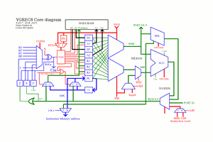
Then I started #AMBAP: A Modest Bitslice Architecture Proposal then #YGREC16 - YG's 16bits Relay Electric Computer then #YGREC-ECL etc. : the new architecture is somewhat simpler and leaner. However the register set's structure is a bit different and not adapted to the concept and organisation of #Discrete YASEP

Then I found out about the 74HC259 (see Enabling discovery) : this circuit (addressable 8-bits latch) is perfect for the bitslice register set. The rest of the circuit becomes a classic design now...


Logs:
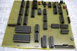
1. First circuits and register set map
2. The ALU
3. Data Memory circuit
4. Parts, parts, parts...

74HC_HCT253.pdf

Datasheet for the 74HC252, a dual MUX4 with tristate output

Adobe Portable Document Format - 748.92 kB - 06/14/2017 at 22:29

Preview
Download

74HC182.pdf

Datasheet for the 4-inputs carry lookahead generator in CMOS

Adobe Portable Document Format - 213.02 kB - 06/14/2017 at 21:24

Preview
Download

mm74hc259-303675.pdf

Datasheet for the 8 bits addressable latch (8×1 SRAM)

Adobe Portable Document Format - 76.87 kB - 06/14/2017 at 20:36

Preview
Download

MC74HC181B1.pdf

Datasheet for the famous 4-bits ALU, in narrow DIP and CMOS version (you can touch it with your fingers without risks of burns !)

Adobe Portable Document Format - 216.98 kB - 06/14/2017 at 20:34

Preview
Download

mm74hc251.pdf

Datasheet for the 8-to-1 multiplexer with tristate output.

Adobe Portable Document Format - 74.80 kB - 06/14/2017 at 20:34

Preview
Download

  • Parts, parts, parts...

    Yann Guidon / YGDES06/16/2017 at 22:08 0 comments

    I received the 74HC181, 74HC182 in record time from deivic ! The same day the 74HC259 arrived too !

    I must dig the project boxes of the #Discrete YASEP to find all the necessary 74HC251, 74HC253, 74HC193 and others I need for this processor. It's fortunate I always purchase extra parts "because you never know !"


    After some "inventorumaging" I have found, in DIP:

    • 74HC153: 80? (need 8, in front of ALU)
    • 74HC157: 9? (needed for some decoding)
    • 74HC253: 80? (need 8, address source select)
    • 74HC259 : ×50 (need 16, one per bit)
    • 74HC245: a lot (2 needed)
    • 74HC573: plenty
    • 74HC273: enough for the output ports
    • 74HC193: plenty (I just need 4, so far)
    • 74HC151: 10
    • 74HC251: 30

    I expected to use 50×'251...

    2 possibilities:

    • use 16×151 for the MUX8, and 32×251 for MUX16 : only 6×151 and 2×251 are missing
    • use the 253 as pseudo-MUX8, the tristate output can be driven by a DEMUX4 (74HC139?)

    Now if I could find a SMD version of the 74HC181, I could almost make a full-SOIC version later :-D however this looks unavailable... I have a bunch of HC283 in SOIC though but that might not cut it, more MUXes will be needed...


    Luckily, the last local electronics parts store in Paris still has some HC parts so I could fill the BOM. I have enough 151 and 251 for a DIP prototype, I added some '154 for decoding the DIP switch array. So I guess it's GO :-)

  • Data Memory circuit

    Yann Guidon / YGDES06/14/2017 at 22:26 0 comments

    The A1,D1,A2,D2,A3,D3 registers emulate a sort of multi-ported memory. However there is only one standard memory chip (or it looks like that with several chips to emulate a 16-bits datapath).

    The circuitry is a bit unusual and requires some MUXes here and there because the result bus can go to the address bus or the data bus of the SRAM chip(s).

    There are two cases to consider:

    • SRAM Write : when writing to the D1/D2/D3 register, so the result bus goes to the Data bus AND the corresponding register latch. The address bus is then controlled by the corresponding A1/A2/A3 register.
    • SRAM Read : the result goes to a A1/A2/A3 register and the address bus. The D1/D2/D3 register is written by the SRAM's data bus.

    So basicly, the SRAM's address bus is selected between the RES bus or A1/A2/A3, that's a MUX4. 8 pieces of 74HC153/253 are required. The 253 adds a tristate output that will be handy for an eventual takeover of the bus for external inspection...

    The SRAM's data bus is bidirectional and a MUX won't work. There are 3 registers connected to the data bus (D1/D2/D3) that can be written by the SRAM or the RES. The SRAM has tristate output and must be isolated from the RES bus. The solution is to separate them with a pair of 74HC573 or 74HC245. The /OE of one is the opposite of the other's /OE to prevent contention.

    So to sum up: the Data RAM part of the system contains

    • 64K × 16 bits of SRAM (probably a pair of Pentium Cache SRAM because they are fast and already available)
    • 2×245 for result bus isolation
    • 6×574 for D1/D2/D3 (let's use 574 instead of 573 because a transparent latch could wreak havoc in the pipeline if the Dx is itself already a source of the address, such as in a linked list)
    • 8×253 for address selection

    That's already a nice board, with 48 bits going from the registers, 48 bits going TO the registers, 16 bits from the result bus and the untold number of control signals...

  • The ALU

    Yann Guidon / YGDES06/14/2017 at 22:07 0 comments

    Contrary to the #Discrete YASEP I'm going the easy route with a fully integrated ALU.

    So it will be the first time I actually USE a 74181 ALU ! After more than a year hearing about it and considering different approaches, this project makes perfect sense. Indeed, there is already a 5-bits field in the instruction for the ALU function, which maps directly to the 181's control signals.

    For now I ignore if I'll use a '182 Carry Lookahead Generator. I like the simplicity of the carry chain system and I don't know if the '182 will significantly speed things up, but the options are open for experimentations (and I'm expecting delivery of the chips in the next weeks...).

    So the 16-bits datapath contains 4×74HC181 (yes, CMOS, not F/S/LS...) and maybe one 74HC182.

    But the function table of the 181 is ... weird ! I'll probably have to make some modifications in the control signals, with a PAL or, if I can, with a 74188 or 74187 PROM. Wait, can I find any similar product ? Can I source some oldfashioned PROM burner ? Or find the specs for burning the equivalent Soviet chips ?

    Let's recap the functions that the ALU of the YGREC are meant to do:

    • Logic group : the whole 16× ROP3 functions, made with a MUX16. I think the 181 does it.
    • ADD/SUB group : ADD, ADDC, SUB, SUBB, MIN, MAX, CMP... ADDC and SUBB reuse the previous carry flag, there are SUB-based comparisons, but the 181 mixes the ADD/SUB logic with ROP2 logic...

    So there is some design to do, to transcode the ALU function into the 181 codes. I've seen others covering it but I didn't bookmark the pages...

  • First circuits and register set map

    Yann Guidon / YGDES06/13/2017 at 21:21 0 comments

    The discovery of the 74HC259 has been an eye-opener. See 35. Enabling discovery

    The heart of the YGREC is its "register set". Actually it's more than a standard register set, it's a sort of hub where data are shuffled and moved around...

    The storage part is built with 74HC259. They are driven with the result bus, as well as the address of the result. One address bit must be a complementary pair to select the right '259. The last input signal is the latch enable, which is sent by the control logic, from the condition result.

    The outputs go to the multiplexers. Well, most outputs, because the registers corresponding to PC, D1 and D2 are ignored, and the outputs for I/O go directly to the output bus.

    Similarly, the MUX will input data from the PC, D1 and D2 latches, as well as the IO inputs. That leaves only 9 bits that are effectively used in the 259s, so maybe if we remove one more register, we can save one 259 per bitslice ?

    Output ports get relegated to 74HC573/4 on a I/O board, for example, hooked to the result bus. The PC, D1 and D2 are also HC573/4s. The last external latch could be a third memory port, D3.

    The new register map is as follows:

    Register name
    (SRCX, DST)
    available
    as SRC
    259
    ?
    Comments
    A1**
    D1*overwritten by RES and DRAM
    A2**
    D2*overwritten by RES and DRAM
    A3*
    D3overwritten by RES and DRAM
    PCPC+1 (some pipelining somewhere?)
    IO1
    IO2
    IO3
    IO4
    R1**
    R2**
    R3**
    R4**
    R5*

    A3/D3 has eaten into the T1/T2/T3 pool so the remaining T is renamed as R5.

    Suddenly, the register map looks more like the YASEP's...

    Not only is the register map heterogeneous, but also the subset addressed by the field SRC is probably not ordered like the field SRCX. This is because the '259 writes to a different set of registers:

    • SRC: A1, D1, A2, D2, R1, R2, R3, R4
    • 259: A1, A2, A3, R1, R2, R3, R4, R5
    SRCSRCX
    259R1, R2, R3, R4,
    A1, A2
    R5,
    A3
    ext. 573D1, D2PC
    D3
    IO1, IO2, IO3, IO4

    Yes it's totally messed up!

    It would be so much simpler if the SRC subset was the whole SRCX set but it's ruled out by the instruction format and the large MUX that is required to make it work... I want the damned thing to be binary compatible with the other generations (relay, germanium, silicon...)

    Anyway, reducing the circuit count is a significant enough saving to justify changing the register map.


    So now that's one '259 per bitslice for the latches, and there are 8 external registers (16×573/4) for the other things.

    • 4×573/4 for the output ports, tied to the result bus. They can be located on a different board for easier manipulations and modularity.
    • 3×573 for the D1,D2,D3 : there will be some steering/buffering of the data bus because the result bus and the R/W bus will talk to each other. This, in itself, will be an interesting log to write...
    • PC comes from 4× '193 but there is some timing issues to consider... another log to write !

    that's 14 '573/4 (I'll decide depending on the timing constraints).


    The inputs : we have a MUX16 and a MUX8, all made from 74HC251. I tried to find a MUX16 but there is no 74HC150 or 74HC250 available in the market (maybe a few LS ones but they require more power and a HCT part later).

View all 4 project logs

Enjoy this project?

Share

Discussions

Eric Hertz wrote 03/31/2018 at 03:06 point

Hah! Was going to say something like "CMOS?! I never thought I'd see the day..." But I see you're using 74HC chips, so, yahknow... TTL part-numbers, anyhow ;)

  Are you sure? yes | no

Similar Projects

Does this project spark your interest?

Become a member to follow this project and never miss any updates