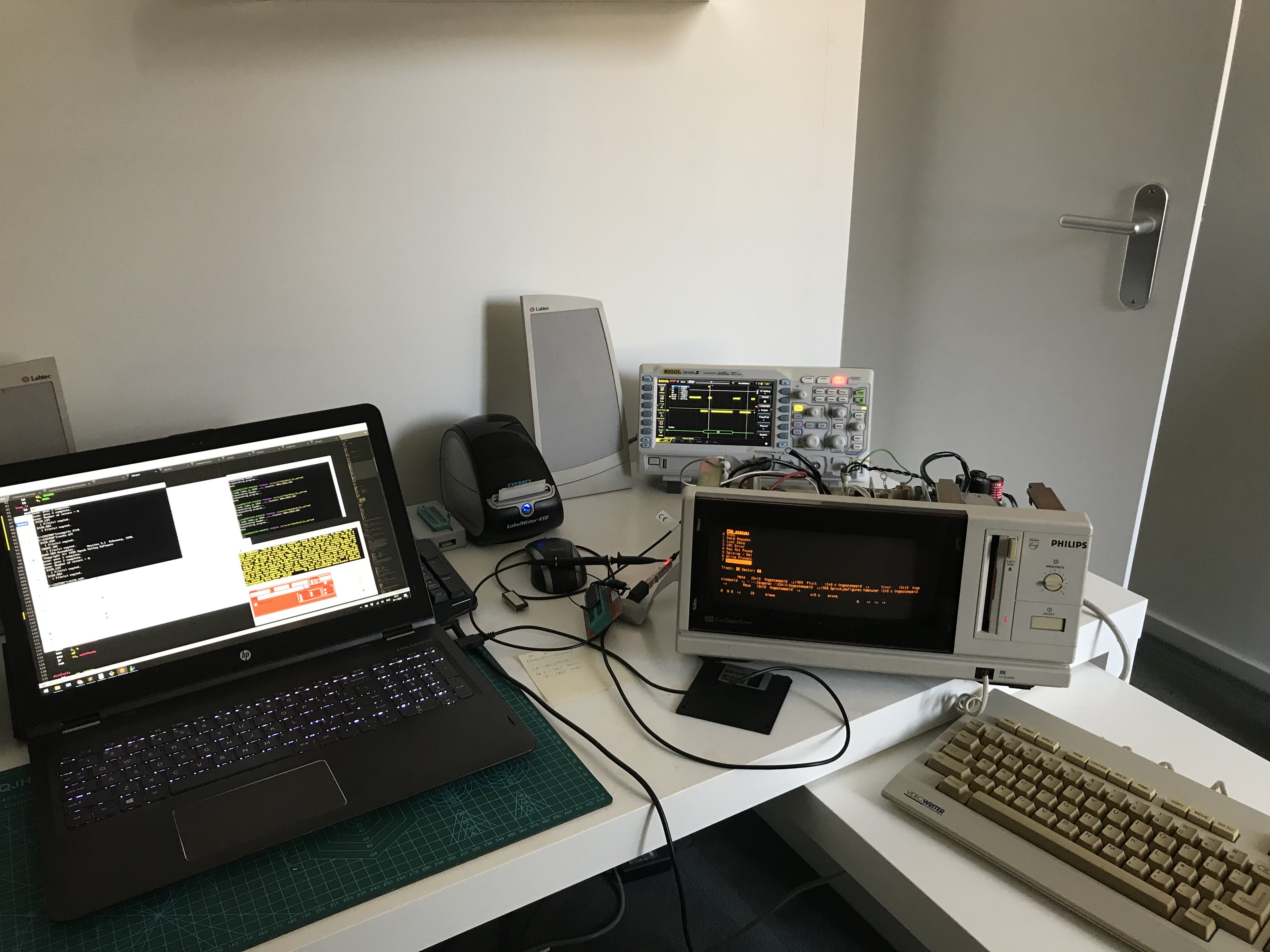
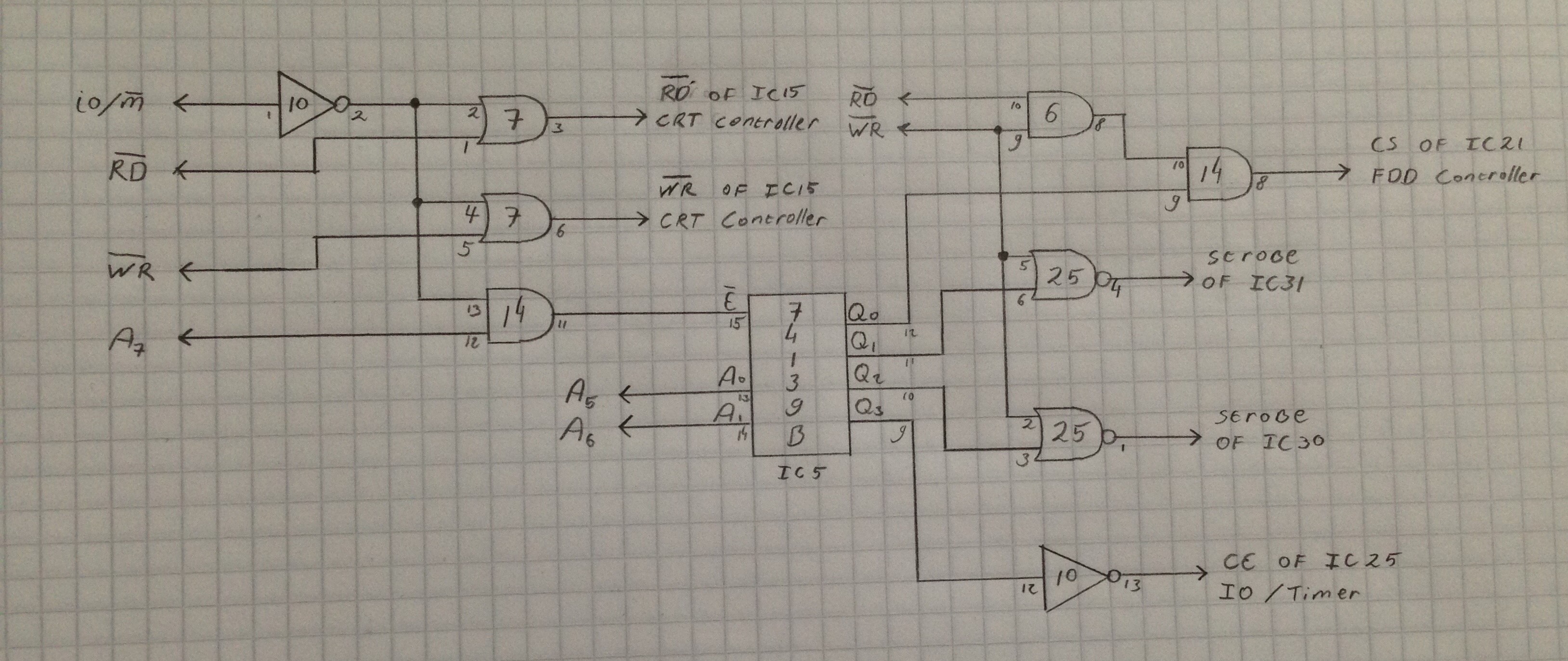
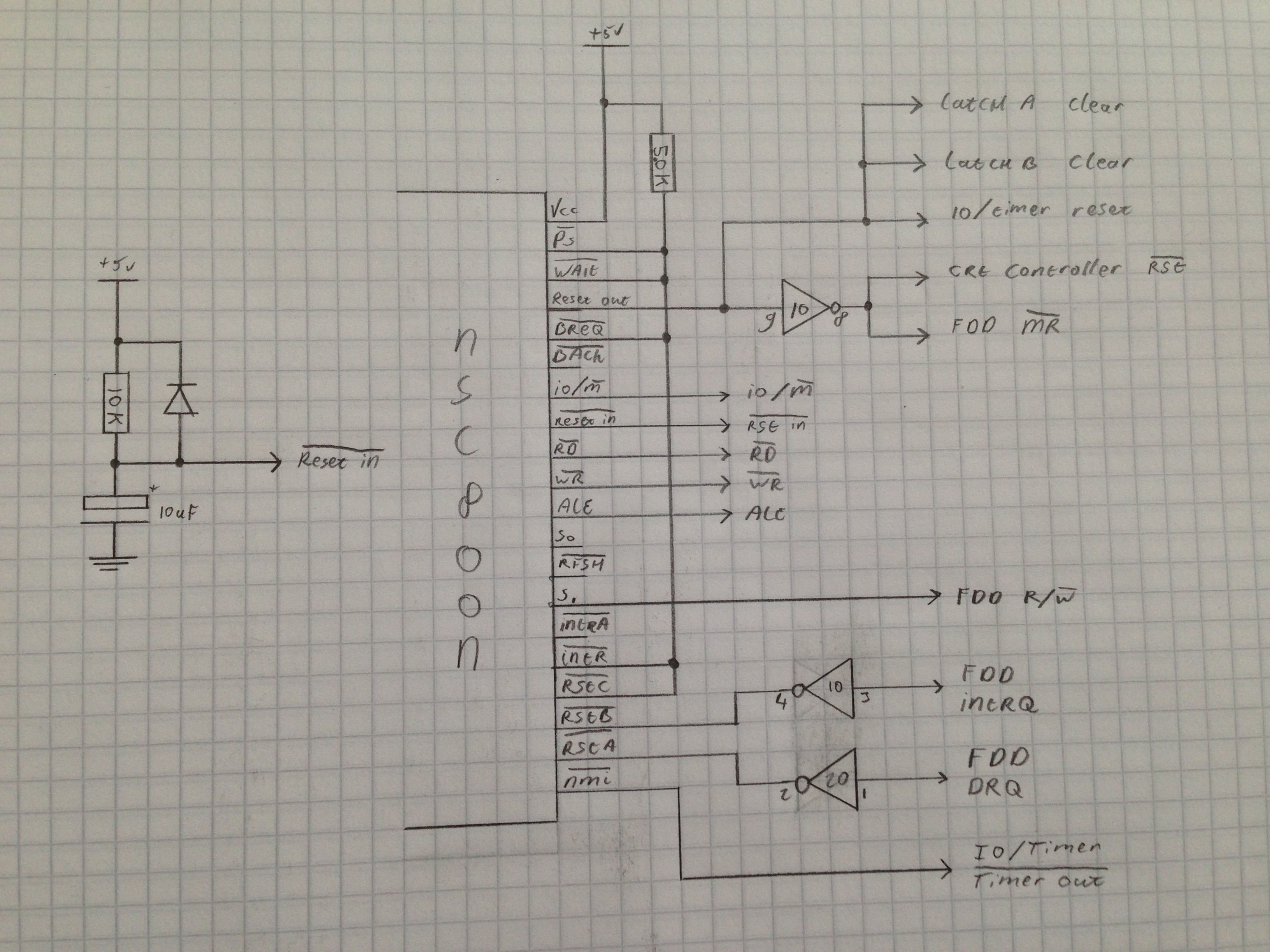
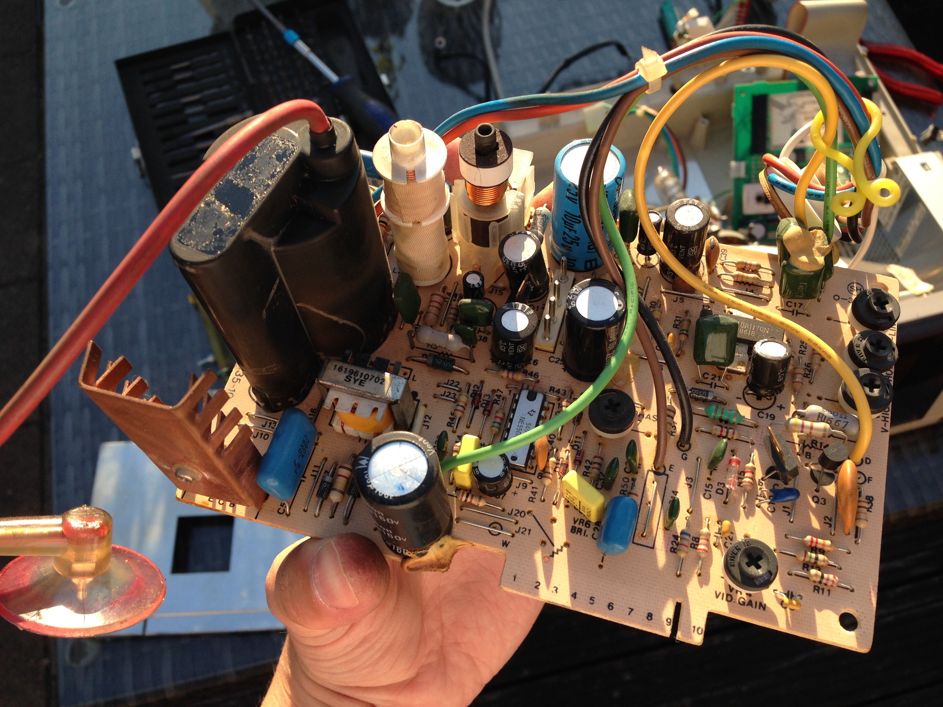
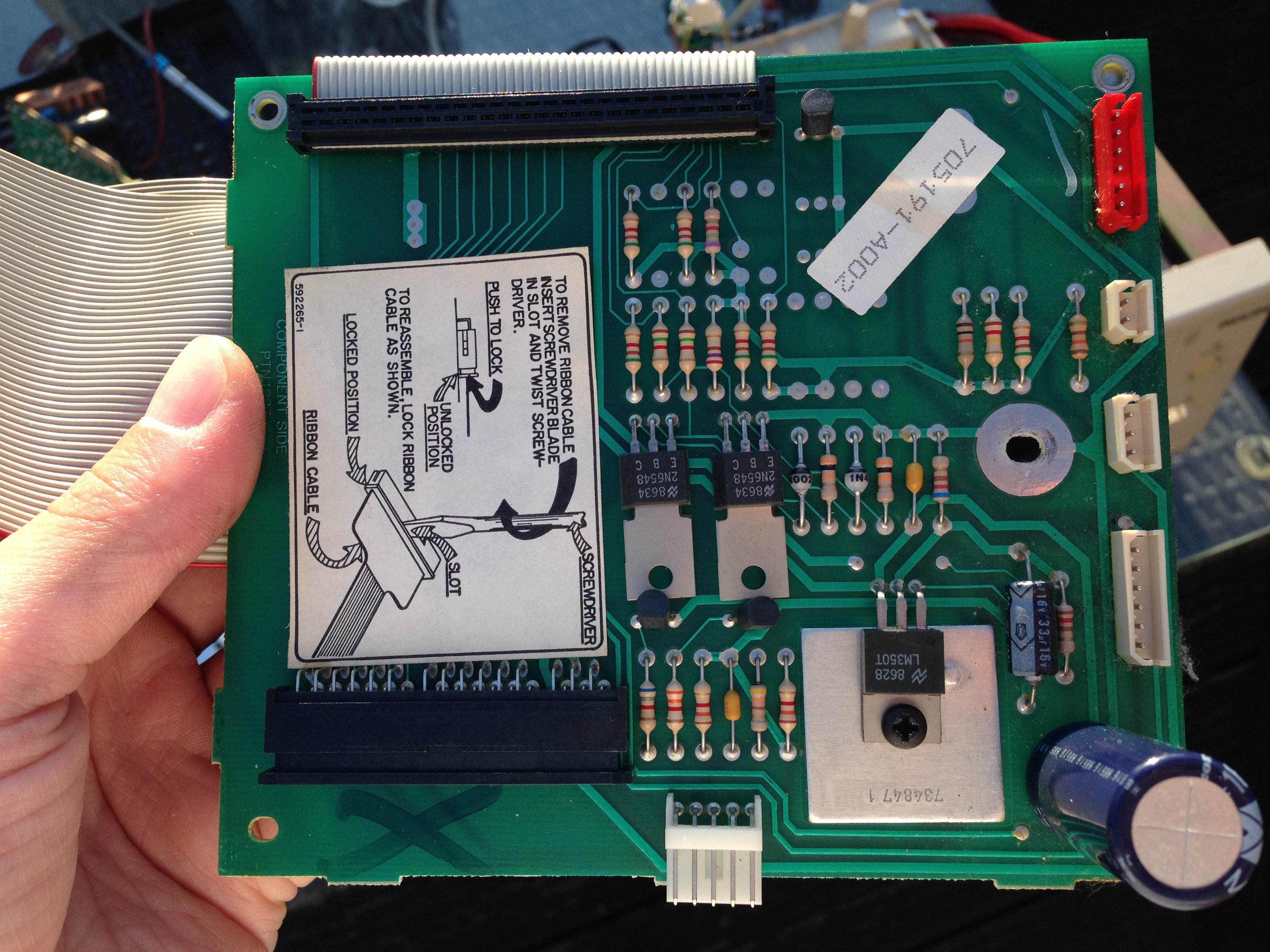
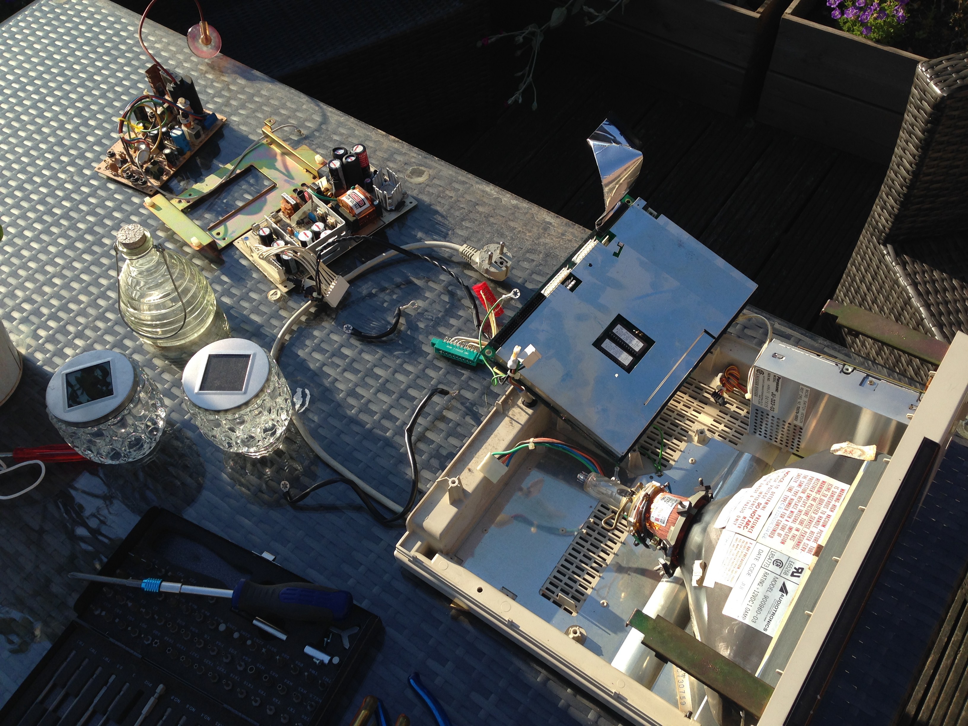
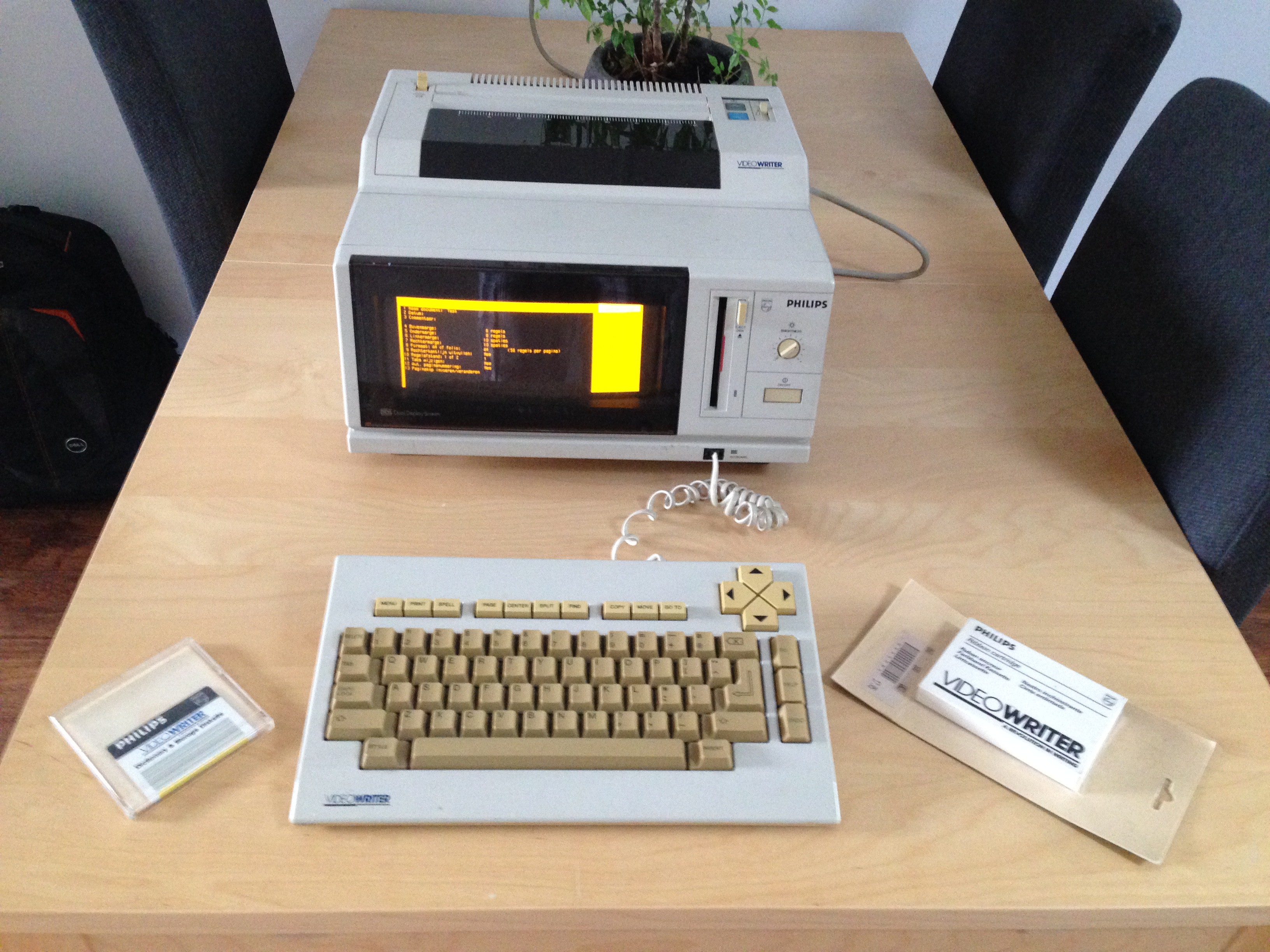
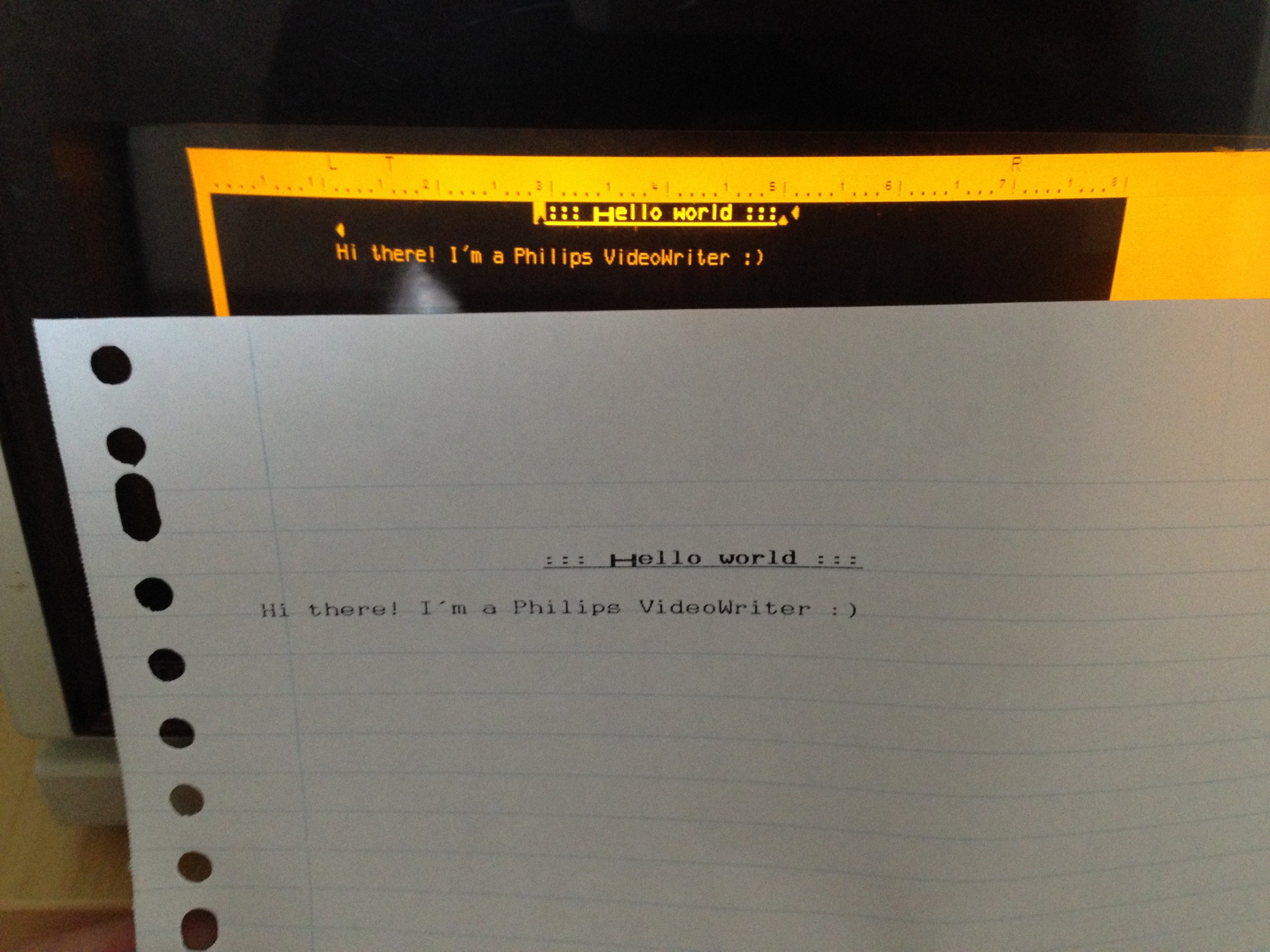
• Disk dumping in progress

    Maarten Janssen01/19/2020 at 12:37 1 comment

    While still working on finishing the documentation for CritterBoot and the display controller I'm also working on the next part of the machine that needs documenting: the disk controller.

    It has been a confusing and frustating process to get the WD1770 disk controller to coopperate. Mainly due to figuring out how the interrupts work and getting te timings to the disk right. But for now I have some routines that allow me to seek and read sectors from the two diskettes I have. I also wrote a quick and dirty serial out that allowed me to completely dump the two disks. 

    Before anyone asks, I'm not going to share these dumps because they contain some very personal documents of previous owners. I will create a new disk with an example document and share its dump here.

    I have no idea yet about the disk format or file format that the VideoWriter uses, but these dumps will be helpful.

  • The Keyboard

    Maarten Janssen12/21/2019 at 17:27 0 comments

    Before I start this log on the keyboard I should mention that I'm in the process of putting all of my writings and software on the Video Writer on a small website. The following is an almost direct copy of what will be the article about the keyboard...

    In this section we'll take a look at the VideoWriter's keyboard and how the unit interacts with it. The keyboard is very nicely layed out with a number of function keys specific to the word processor, for example to do spell checks or to get access to contextual help screens. Inside the keyboard we find a NEC D8049HC microcontroller. It has 2KB of program ROM and 128 bytes of RAM. The microcontroller scans the keyboard switches and handles the communication with the VideoWriter. A nice surprice was to find that it also implements a FIFO buffer that can hold up to 20 keystrokes. If this buffer is full then no more keys will be added until one is read out. When holing a key down it will start to repeat after a short delay as you would expect.

    Read more »

  • A Video Writer Holiday Card

    Maarten Janssen12/16/2019 at 21:40 1 comment

    After a long period of inactivity I'm back working on the Video Writer! More will come soon, but here is a very short progress update:

    • I understand how the video chip works and mostly documented
    • The keyboard has finally been demystified and fully documented
    • I have actual serial communication working (No more faking it with an Arduino )
    • I made a custom ROM that allows me to upload and run my own code!

    The holiday card below is a screenshot of a little program I wrote and uploaded to the VW

  • Decoding the I/O and CPU signals

    Maarten Janssen07/28/2017 at 18:54 0 comments

    It's time to start looking at the IO map of the VideoWRITER. With the help of my trusty multimeter I have been probing around the main board and I've drawn the following schematic.

    Let's start looking at the left part of the schematic before the 74139. This is where the /RD and /WR signals for the video controller (VDP) are generated. Notice that there is no chip select signal for the VDP in this schematic. This puzzles me since the only signal going to the VDP that comes close to a /CS signal is the CPU's ALE. But that means that any IO operation also ends up at the VDP as far as I can tell now. Let's park this for now and continue with decoding the rest of the IO.

    The rest of the IO addresses are decoded using the second half the 74139 we saw before when decoding the memory. This half of the 74139 is enabled when we're doing an IO operation and A7 is low. It looks like A7 is responsible for choosing between addressing of the VDP and other IO. A6 and A5 determine the device that is selected by the 74139. This decodes to the following:

    A7A6A5Selected device
    000Floppy Disc Controller (FDC)
    001Latch B (IC31) only when /WR is active also
    010Latch A (IC30) only when /WR is active also
    011IO / Timer (IC15)
    1xxVideo Display Controller (IC15)

    Just a thought... Could A7 be used as an active high chip select line for the VDP? It's hard to tell without the datasheet of the NCR 7250, but it would make sense unless there is some magic happening with the ALE line going to the VDP chip. This is something to look into for the next log...


    CPU Signal Lines

    While we're at it let's take a closer look at the signal lines coming from and going to the CPU. That allows us to say something about the various interrupts that are generated in the system as well. Once again I buzzed-out the schematic and drew it on paper.


    Reset

    Starting off with the reset circuitry, the CPU has a /RESET IN and RESET OUT line. The /RESET IN line is what resets the system when pulled low. The inverse of this signal is put on the RESET OUT line to generate a reset pulse for the various devices connected to the CPU. In our case it resets all the IO chips FDC, VDP, IO / Timer and Latches when power is applied.


    Interrupts

    Let's continue at the bottom of the chip now where the various interrupt signals come in. Starting off with the /NMI (Non Maskable Interrupt) pin. The NMI works the same as for a Z80. When interrupts are enabled and this pin is pulled low the CPU will jump to an interrupt service routine at address 0x66. In case of the VideoWRITER the /NMI signal comes from the timer output of IC25 (IO / Timer). Every time the timer rolls over an interrupt is generated.

    In addition to a Z80 compatible /NMI the NSC800N also has a Z80 compatible mode 1 interrupt that jumps to 0x38 when /INTR is pulled low, but this is not used in the VideoWRITER.

    Besides these two interrupt signals the NSC800N has three restart signal inputs /RSTA, /RSTB and /RSTC that make the CPU jump to 0x3C, 0x34 and 0x2C respectively. The VideoWRITER uses the first two and they are controlled by the floppy disc controller. With /RSTA the FDC tells the CPU about the status of its data register and /RSTB tells the CPU that the FDC has completed its last command.

    Machine states

    The final signal I want to highlight is the S1 line. Together with S0 these determine the bus status. As you can see this controls the R/W line of the FDC. But why is S1 used instead of the /RD and /WR lines only for the FDC? This is not clear to me. Using the S0, S1 and IO/M lines is probably the intended way of decoding memory and IO read / write states, but using other lines has the same effect. Maybe the designers were just trying it out and said 'screw it!' for the other devices and went with a Z80 like way of decoding read / write states. Anyway at the NSC800N datasheet and the table below it shows that S1 can be used as an IO read signal, but only if there is also an IO select signal going to the device.

    S0S1IO/M/RD/WRMachine Cycle...
    Read more »

  • Investigating the ROM and RAM

    Maarten Janssen07/09/2017 at 17:48 0 comments

    Continuing my VideoWRITER autopsy, this time I want to learn more about its memory configuration. Last time we already saw that the system holds 16kb of RAM and a total of 64kb of ROM, leading me to believe that we may also find some bank switching circuitry today. I did some poking around with my multimeter on continuity to trace the various signals and drew some schematics on paper.


    Chip Selects

    I will start by reverse engineering the chip select lines of the memory. This should give us a rough idea of the system's memory map as well since usually a particular memory chip is selected based on its address in the memory map. I will start from the /CE pin of ROM A. Running the other probe of my multimeter along the pins of other chips on the board until I hear a beep. And hey, what do you know it starts beeping at the output of an AND gate. Now to trace the two inputs of this gate... Turns out they go to two outputs of an 74139 (a 1 out of 4 selector).

    The 139 has A14 and A15 from the CPU as its address inputs, so this means that the memory is divided up into four blocks of 16kb. The /E (enable) line of the 139 goes to the CPU's /M (memory select) line, so the 139 is active when the CPU wants access to the memory. After tracing the circuit I come to the following memory map in the table below. ROM A is active when either /Q1 or /Q2 of the 139 is active, ROM B is active on /Q2 and the RAM on /Q3, but the RAM is not as straightforward as the ROMs. More on that later...

    A15 A14 Memory
    0 0 ROM A
    0 1 ROM A
    1 0 ROM B
    1 1 RAM


    The Address Bus

    Address bus schematic

    Let's now take a look at the address bus of the VideoWRITER, because it's a bit more involved than that of a normal Z80 system. As I noted last time the NSC800N shares the lower half of its address bus with its data bus. So in order to separate the two what they did was use a 74373 (an 8-bit latch) to hold the lower 8 bits of the address bus. The inputs of the 373 connect to AD0 through AD7 of the CPU and the CPU's ALE line is connected to the latch pin of the 373. Thus when the CPU's Address Latch Enable line goes high the lower half of the address is copied into the 373. The /OE of the 373 is tied to ground, so it's always holding the current address on its output.

    From now on I will refer to the address bus as the combined output of the 373 and upper address lines of the CPU as A0 through A15.


    ROM Addresses

    Now we know how the address bus is set up we can take a look at how the ROMs are connected. Starting with ROM A we find nothing unusual. A0 through A14 are tied together as you'd expect. For ROM B A0 through A13 are tied to the address bus, which makes sense since it can only use 16kb according to the memory map we found earlier. What about A14? Does it go to Vcc or ground to disable one half of the memory? Nope. It goes to pin 39 (PC2) of the D8156 IO controller. That means that the upper and lower 16kb of ROM B can be exchanged in software and the bank switching mystery is solved :).


    RAM Addresses

    This is going to be the complicated part of this log. We saw that the VideoWRITER uses two 16k x 4 DRAM chips for its RAM. We also saw that in order to make a full 8-bit data bus one chip serves the upper four bits and the other the lower four. This means that all the signals going to the chips are the same for both.

    To select an address of these DRAMs you need to first select a row address, followed by a column address. In this design this is implemented using two 74157s (2 to 1 line data selectors). These are used to output the row or the column address depending on the select input. To know when the row or column is selected we have to go back to schematic 1. Above the RAM /WR output you see that there is another output going to the select line of the first 157. Following the logic gates from the schematic, worked out below, we can deduce that when /Q3 is low a column address is selected and when /Q3 is high a row address is selected. ...

    Read more »

  • 3. The Main Board

    Maarten Janssen07/03/2017 at 18:44 0 comments

    This time to take a look at the main board of the VideoWRITER and take a first guess at how it works. Let's take a closer look at the 7 big chips in the middle row of the board rom left to right. I added the datasheets of all chips (when available) to the project page.

    VideoWRITER Main Board


    D8156HC-2 - IO controller

    This is probably the controller for the printer, judging by its location on the board relatively close to the printer connector in the top left corner of the board. This chip has three I/O ports (two of which are 8-bit and one 6-bit wide), a 14-bit timer and 256 bytes of static RAM. I hope to find out later what each of the ports on the chip is used for and confirm that it's used to control the printer. It's probably also used to communicate with the keyboard. The 8156 uses a combined address and data bus just like the CPU, as we will see in a bit.


    HN27C256-20 - 32kb x 8 EPROMs

    The next two chips are two 32kb EPROMs that contain the VideoWRITER software. This brings the total to 64kb of ROM, which contradicts the Wikipedia article that states that the system only has 16kb of ROM. This amount of ROM also suggest that there is probably some bank switching going on if the full 64kb is used. That is beacause the CPU , which is going to be a Z80 clone, can only address a maximum of 64kb of memory and there must be some RAM on this thing as well. Spoiler alert: there is 16kb of RAM. So maybe one of the ROMs is being bank switched to select either the upper or lower 16kb of ROM to leave room for the RAM. We will investigate further in a later log...


    NSC800N-3I - CPU

    NSC800 vs Z80 Pinout

    Yes, this is a Z80 clone. However it is only a clone in a sense that it has the same instruction set. The pinout of this chip is completely different of a normal Z80. The pins on the left side of the device are all the address and data lines neatly ordered. The NSC800 has a combined address and data bus. This means that the lower 8-bits of the address bus are also used by the data bus. To select between the two the CPU has an ALE pin that is high when these 8-bits are to be used as the lower 8-bits of the address. The right side of the chip is completely dedicated to control signals like ALE, Read Enable, Write Enable, Memory / IO selection etc. It looks like this CPU is probably going to be harder to work with than a regular Z80, but also this is something we will find out later... From the datasheet we can see that the CPU runs at 2.5MHz, which means that the 5MHz clock from the nearby crystal must be divided by two somewhere.


    HM48416AP-15 - 16kbx4 DRAMs

    Next we take a little side track to take a look at the two DRAM chips below the CPU. These are two 16kb DRAMs with a 4-bit wide data bus. It makes sense if one of these serves the upper 4-bits of the CPU data bus and the other one servers the lower 4-bit half. So it wouldn't surprise me if I will later find that the address lines of these chips are tied together to form a combined 8-bit data bus.


    WD1770-PH - Floppy disk controller

    Now this is an interesting chip! We are looking at a Western Digital floppy disk controller. This chip apparently needs only a minimal number of external components to communicate with a floppy disk drive and it can also format floppies using various formats. This short description is not doing it justice, so it's definitely something for a later log.


    NCR 7250 PY - Display controller?

    For this next one all my searches have come up empty. I don't know yet what it is, but I'm fairly sure we're looking at the display controller here, since it's the only major component still missing.


    HM6116-4 - 2kb x 8 SRAM

    More RAM? This is probably used by the nearby display controller as its video memory. The display is probably not a bitmap display, but rather character mapped. This means that the RAM will contain the character codes of what is shown on screen and that the display controller maps these codes into a pattern to show on screen using its internal font bitmap. The size of 2kb seems a bit small though,...

    Read more »

  • 2. Take it apart!!1!

    Maarten Janssen06/28/2017 at 20:27 4 comments

    Let's start taking apart the VideoWRITER and see what boards we will find. I won't go into too much detail on the boards in this log, just a quick first look at them.

    After removing the cover let's start by discharging the CRT. It probably holds little to no charge since it's been switched off for a while, but I'd rather be safe than sorry. I have my trusty screwdriver connected to a length of thick wire and an alligator clip at the other end for this job. I connect the aligator clip to some of the metal frame and squeeze the screwdriver under the anode cup of the CRT. No clicks or pops from this one that suggest a charge, but I always repeat this process at least ones after a minute or so just to be safe.

    Inside the VideoWRITER


    Power Supply

    Ok now we can safely start touching things and taking the boards out. First up is the power supply. Just two screws to remove here and the PCB comes out. I should mention that this is the second time that I remove the power supply. When I was testing the VideoWRITER a couple of weeks ago before putting it up for sale one of the caps violently exploded. There was a lot of smoke and that special smell of burnt electronics. Luckily I had a spare cap in my parts bin so I was able to replace it (it's the red cap in the top middle of the board). The power supply was working again, but whether there are still other problems with this board that caused the cap to blow is still a mystery.

    Power supply board


    Monitor Chassis

    The monitor chassis almost made me go "aww that's cute" just because it's such a small and simple looking board compared to other monitor chassis's I've seen. Of course it's just a monochrome CRT, but for example up to now I've only seen assemblies where there is a neck board that plugs into the CRT instead of just a plug. Also all the common adjustment pots for the video signal are there. The board has a 10 pin edge connector that connects to the main board of the VideoWriter. It would be interesting to see what the pinout is of that one. What intrigued me was finding a 556 (dual 555) timer chip on the board. Maybe for some video signal timing?

    Monitor Chassis


    Printer Interface

    This board was actually not found under the cover, but directly under the printer mechanism. It's not very interesting I think. It connects from the main board through a big ribbon cable and from there goes to the motors, paper feed buttons, printing contrast slider, cartridge cradle, end stops and paper sensor. I'm just stalling for the best part...

    Printer Interface Board


    Main board

    The main boad of the VideoWRITER is very interesting I think. I will spend the next logs on it. For now enjoy the board still covered by its shield and the other components spread over the garden table. But you can tell that there are at least two rom chips on the main board peaking throught the shielding. You can also see what remains in the unit: the CRT and the floppy drive.

    Guts Spread Out


  • 1. History

    Maarten Janssen06/26/2017 at 20:14 0 comments

    First let's start off with some history or introduction of the VideoWRITER, because knowing myself if I don't write this now I never will.

    The VideoWRITER is a word processing machine with built-in screen and printer introduced in 1985. Supposedly it runs on a Z80 clone and has 16kb of ROM and 16kb of RAM. Documents are stored on 3 1/2" floppies. When it was new it was sold for $799.

    My VideoWRITER

    The screen is a monochrome amber display that is noticeably wide. When the machine is turned on it is split into two halves. The left half that shows the text editor, settings and document properties and a sidebar on the right that shows you menus, hints and the functions of special keyboard keys. Also the sidebar is always in inverted video to make is stand out. I guess that that's what they mean with the 'DDS - Dual Display Screen' in the bottom left of the screen cover.

    Editing documents is very basic by today's standards, so don't expect any fancy fonts such as Comic Sans ;). There is only one built-in font that you'll have to make due with. Changing the font is actually just changing the text style to bold, italic, underline, sub- or superscript. Other layout options include text alignment and... that's all. Apart from that the editor shows a ruler at the top of the screen and special characters such as new lines are also shown.

    It prints on standard A4 paper using special ink ribbon cartridges and some thermal printing process. According to the Wikipedia article you can also use it as a thermal printer when you print on thermal paper without the cartridge. I was quite surprised that my VideoWRITER was still printing after many years in a warm attic.

    It still prints!!1!

    The keyboard is small, yet comfortable to type on. It has a number of special keys that allow you to change the font, undo, or do a spell check (if you have the diskette that contains the dictionary that is). The keyboard connects to the main unit using an RJ14 phone style connector.

    Documents are saved on 3 1/2" floppies. The machine will look for one when you switch it on and ask you if it's ok to format it if necessary. I don't think the VideoWRITER floppies are formatted to be PC compatible and probably can only contain 360 kb, or 720 kb at best. Maybe we will find out later.

    Next time let's lift the cover and see what we find.