 Pavel
PavelThese are models of memory devices, with essential wiring which may be implemented in full-scale devices, but otherwise shrunk to bare minimum, just to test the idea.
First of these are two one bit registers, connected via bus.
It is subproject for the one devoted to dispay. Here I will focus on memory elements.
Already have an account? Log in.
To make the experience fit your profile, pick a username and tell us what interests you.
These are models of memory devices, with essential wiring which may be implemented in full-scale devices, but otherwise shrunk to bare minimum, just to test the idea.
First of these are two one bit registers, connected via bus.
|
Adobe Portable Document Format - 240.15 kB - 07/12/2017 at 07:29 |
|
|
Here is the video of the second prototype in action:
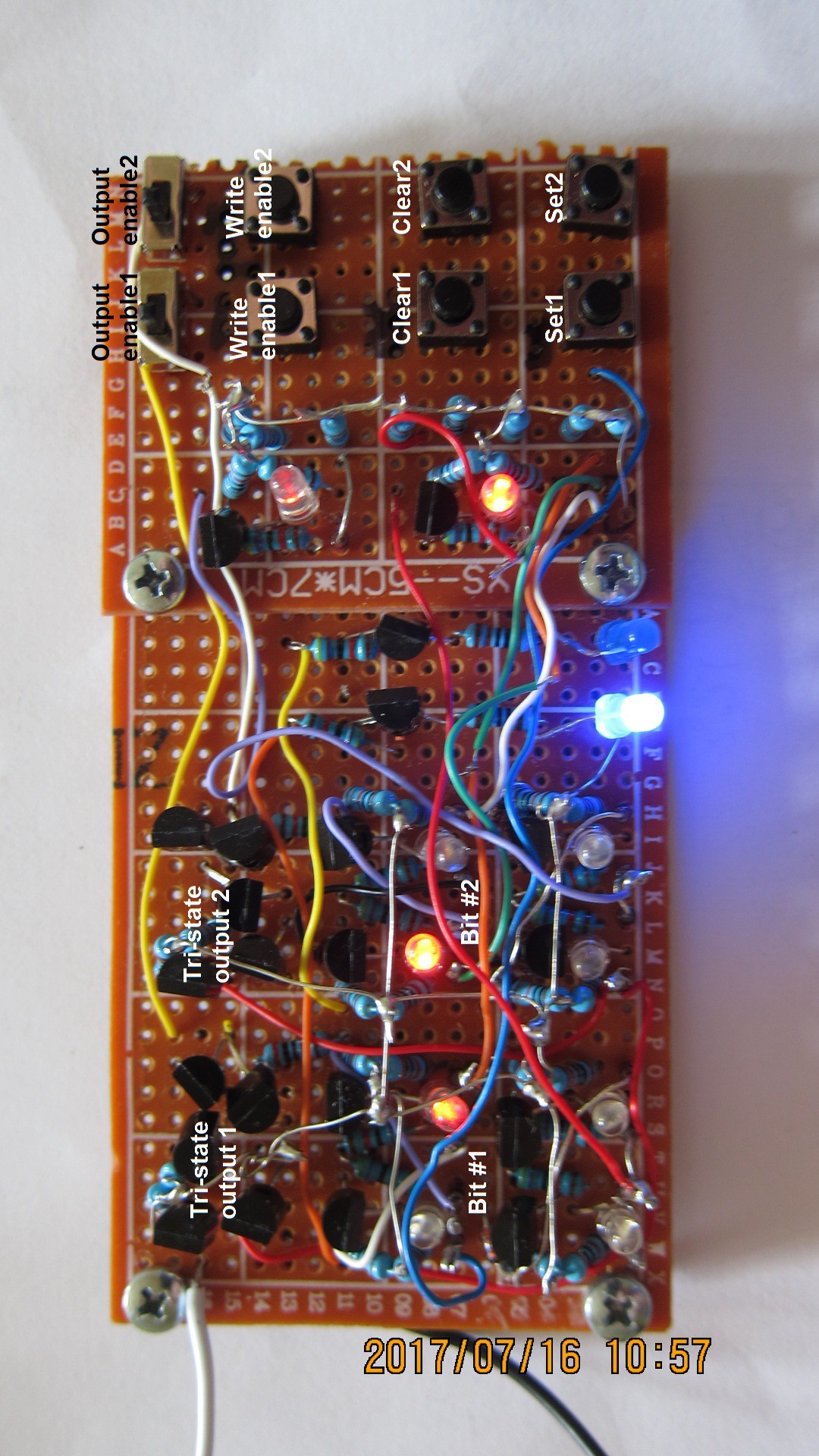
The switches and buttons are marked and there is the meanings, left to right:
S: source address, enables addressed register onto the bus;
D: destination address, enables writing into addressed register fron bus or setting it to 1;
Write: performs writing from bus into register addressed by pair of switches marked as D;
Set: pushing this button makes register addressed by D set to 1;
R: resets all registers to 0.
Source and destination addresses are indicated by pairs of yellow leds, contents of registers are indicated by row of blue leds, registers numbered from top to bottom 0 through 3.
The assembly took longer than expected, but now the complete system works as it should. Main hindrances to completion were, aside procrastinstion, apperent lack of time due to personal life issues, and -- bigger problems was mystery short-circuit (remedied by slightly bending the board) and misapplication of epoxy resulted in stuck switches. The latter problem was solved by making and attaching small board with new switches.
Here is photo of prototype working (photos were made before epoxy misapplication):
I hope in several days I add a video of the thing working. For nearly month I am not going to build new devices because of transistor shortage - a new batch should come in a month, approximately. For now I am going to reevaluate my logic gate design, to see what can be done to make them faster with at least the same reliability. Maybe even use less parts per gate?..
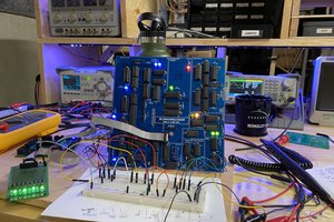
The four-registers system is almost conplete, two boards assembled, tested and debugged and are working as expected. The only thing yet to do is to connect the boards propery, and hopefully it will be done without additiinal trouble. Here is how it all looks like as of now:

On the left half are the registers themselves, and in the corner is support circuitry for register contents indicators (blue leds in the same corner of right half). On the right board are control circuits -- switches and buttons, and three 2-to-4 decoders (demultiplexers) for choosing the registers I want to do operation on. There is circuitry for choosing which register to set to 1, to enable to be written to from bus and which to enable output to bus. Reset is global and is applied at once for all registers.
As was stated in previous log, I plan to build model register system, which is next level of complexity, as it is will have addressable registers and also less controls compared to previous system (7 vs 8). Here is schematics for it:
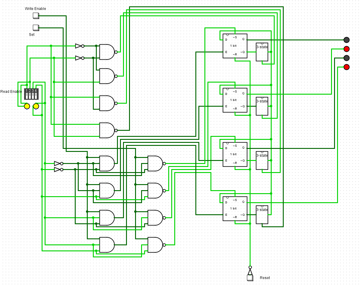
There is no option in this system where bus can float, as it always has one of the tri-state outputs open (exactly what output is open is dictated by 2-bit address, first two spdt switches). This model also have global reset, but each register can be set individually via 2-bit address (last two spdt switches), or written to using the same address.
Well, now I have to make it in hardware!
I completed construction of my first model, have tested it, and it works as it should. Here is how it looks complete:
And here is schematics:

Having accomplished this first goal of making proof of concept, I am going to take the next step - making model system consisting of four 1-bit registers on the same bus. But now it will not only be mere scaling up of above model, but the registers should be addressable, the model should have controls for choosing the source and destination registers and for setting them up properly.
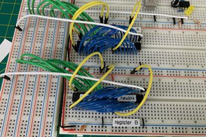
Today I ended building the main board for this little device. The thing consists of two one-bit registers, connected to common bus via tri-state outputs. The schematic is as this:
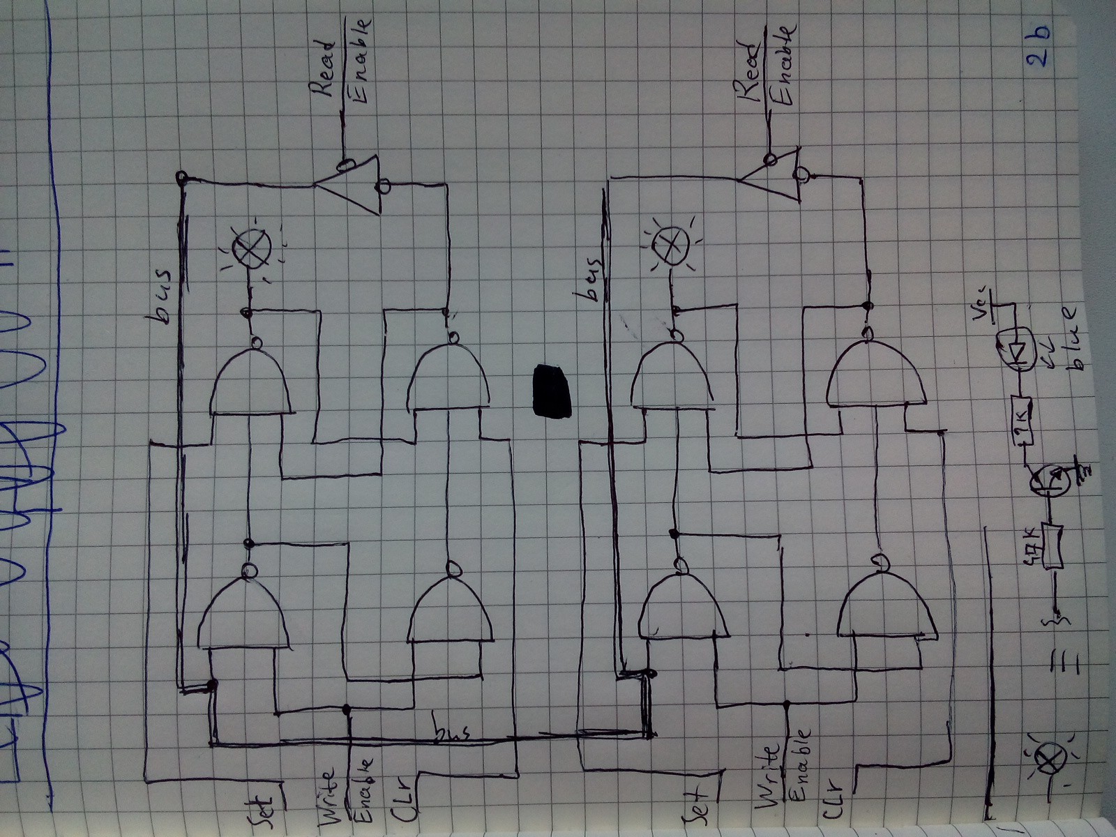
As one could see, the memory elements are resettable transparent d-latches, made of four NAND gates each.
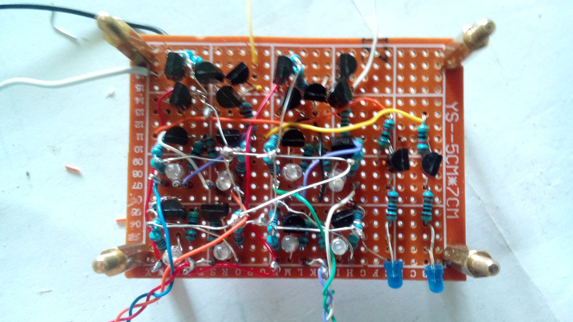
Here is how the board looks like:
Also, there is an annotated image saved as pdf file.
The board seem to work. There is other one pending - the board with all needed controls, so as to be able to handle these registers properly and be indeed sure if it's working as intended. As of now, all these hanging wires are a mess.


 Grant Giesbrecht
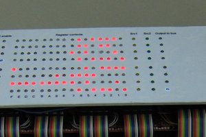
 Brandon Reinhart
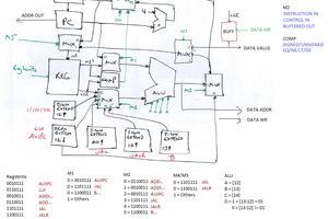
 Phil Wright