0%
0%
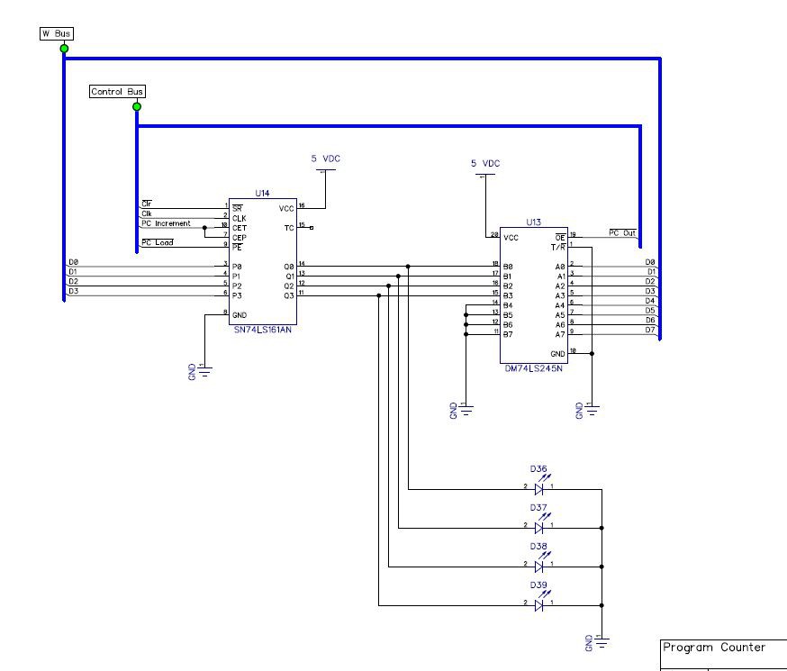
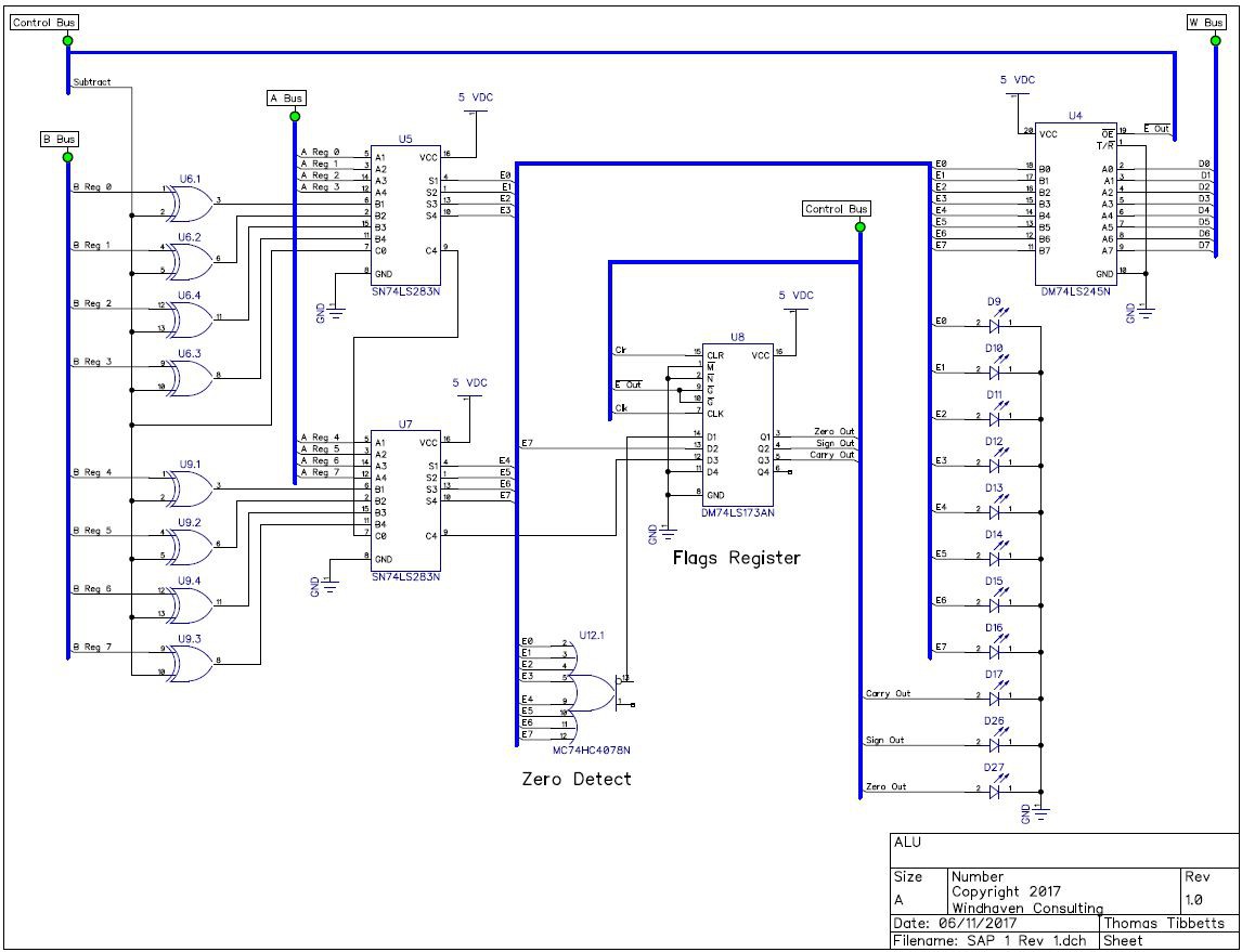
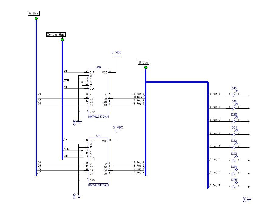
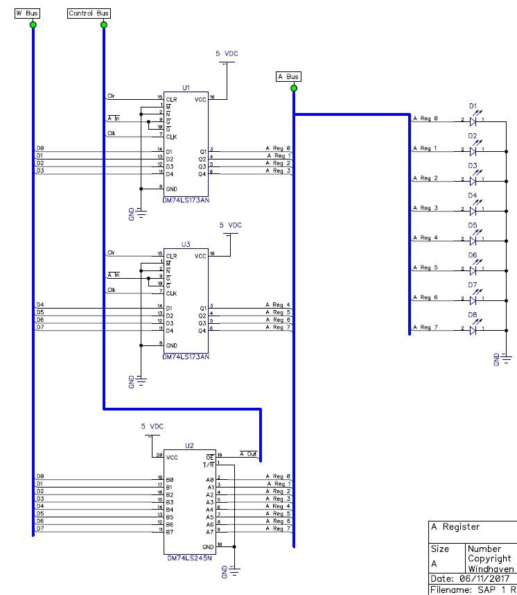
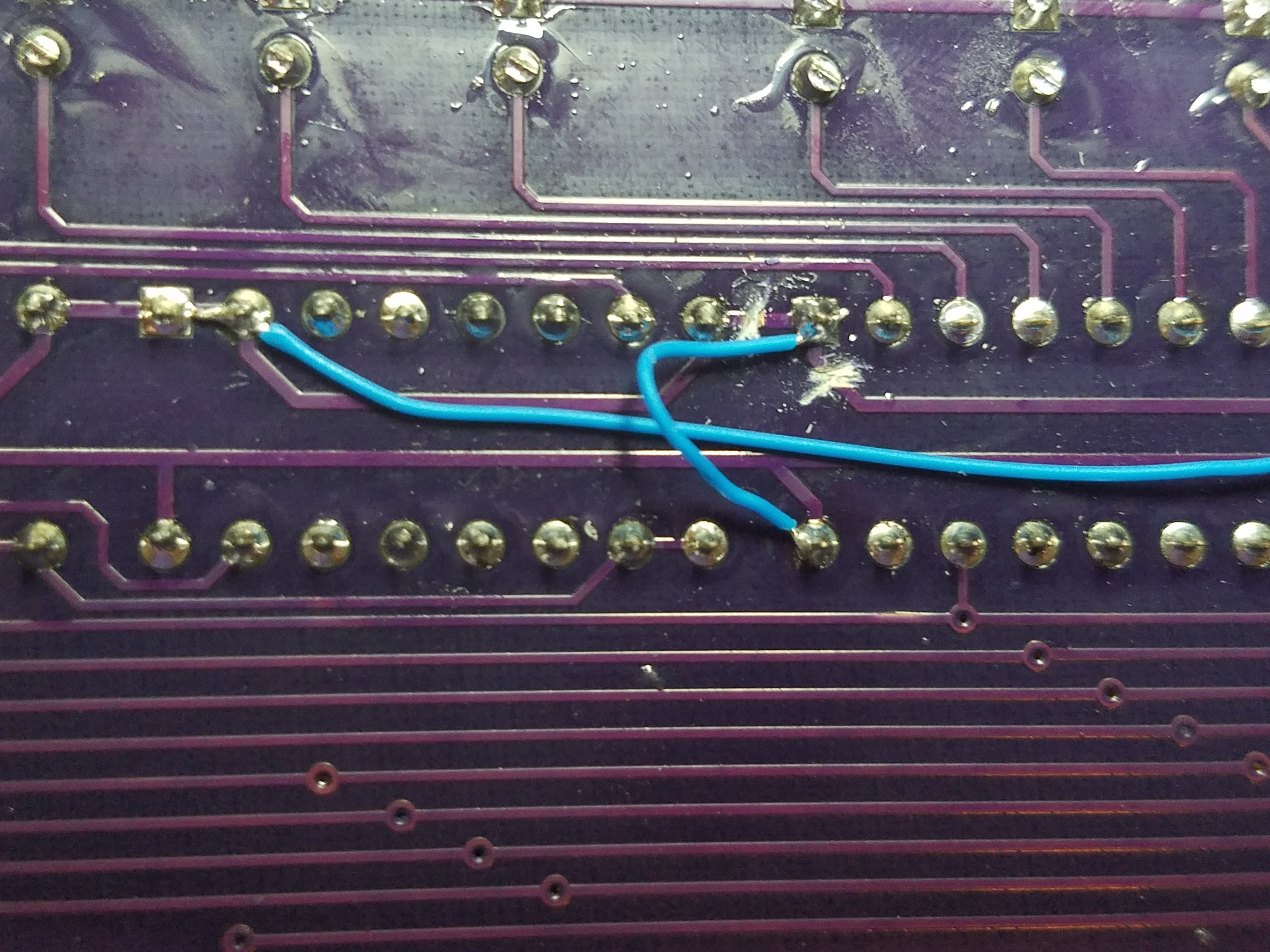
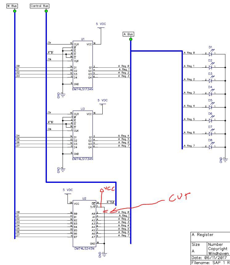
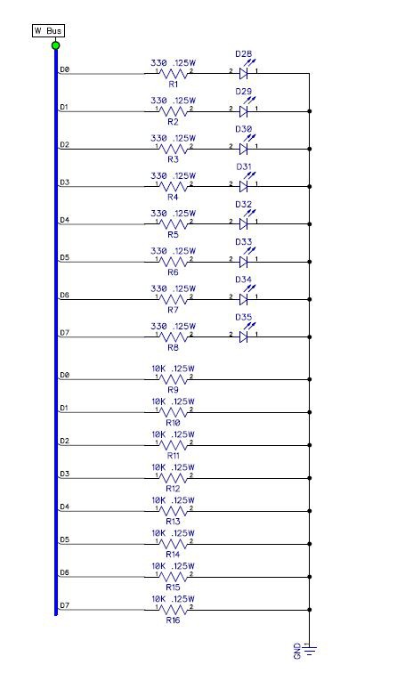
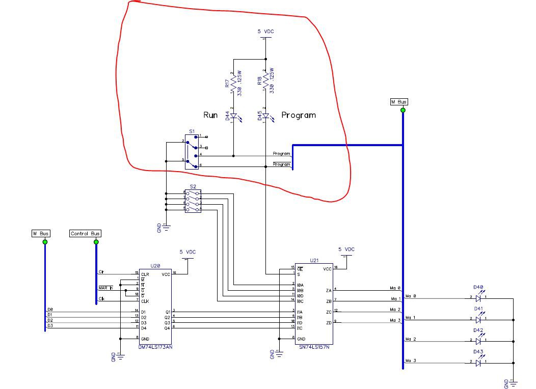
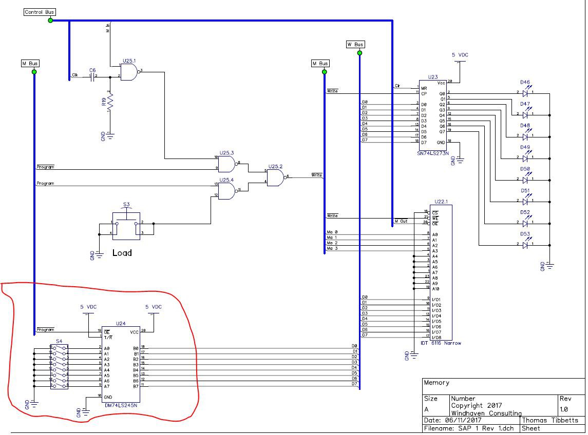
SAP 1 Computer on Printed Circuit Boards
Inspired by the video series by Ben Eater, I am developing a set of printed circuit boards for the simple as possible computer.
 tomtibbetts
Become a Hackaday.io member
Already have an account? Log in.
Just one more thing
To make the experience fit your profile, pick a username and tell us what interests you.
Pick an awesome username
hackaday.io/
Your profile's URL: hackaday.io/username. Max 25 alphanumeric characters.
Pick a few interests
Projects that share your interests
People that share your interests


 matseng
 Dr. Cockroach
 Pavel
Pavel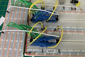
 Brandon Reinhart
Hi,
I'm new here. I love this project. I have been doing Ben Eater CPU project for a while now, but I would really like to solder it together rather than doing it with breadboards.
I am also new at electronic. How would I go about taking your design in the pdf files and ordering PCBs? Can I even do that from pdfs?
Best regards,
Mads Ravn