 tomtibbetts
In this, step two, we are building out the A Register. The A register is used as the accumulator for the computer and, as such stores the results of additions and subtractions. We will be using 8 red leds, 2 74ls173s four bit registers and 1 74ls245 bi-directional tri-state buffer. Here is the section of the schematic we're building:
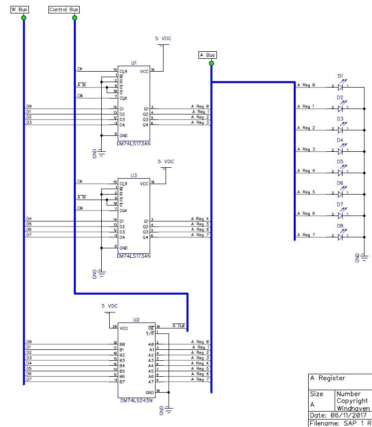
Of note are the control lines: Clr (for resetting the register to zero), Clk for latching a new value into the register, ~A In, to enable the register to load new data, and ~A Out for moving data from the A Register to the W Bus which we built earlier.
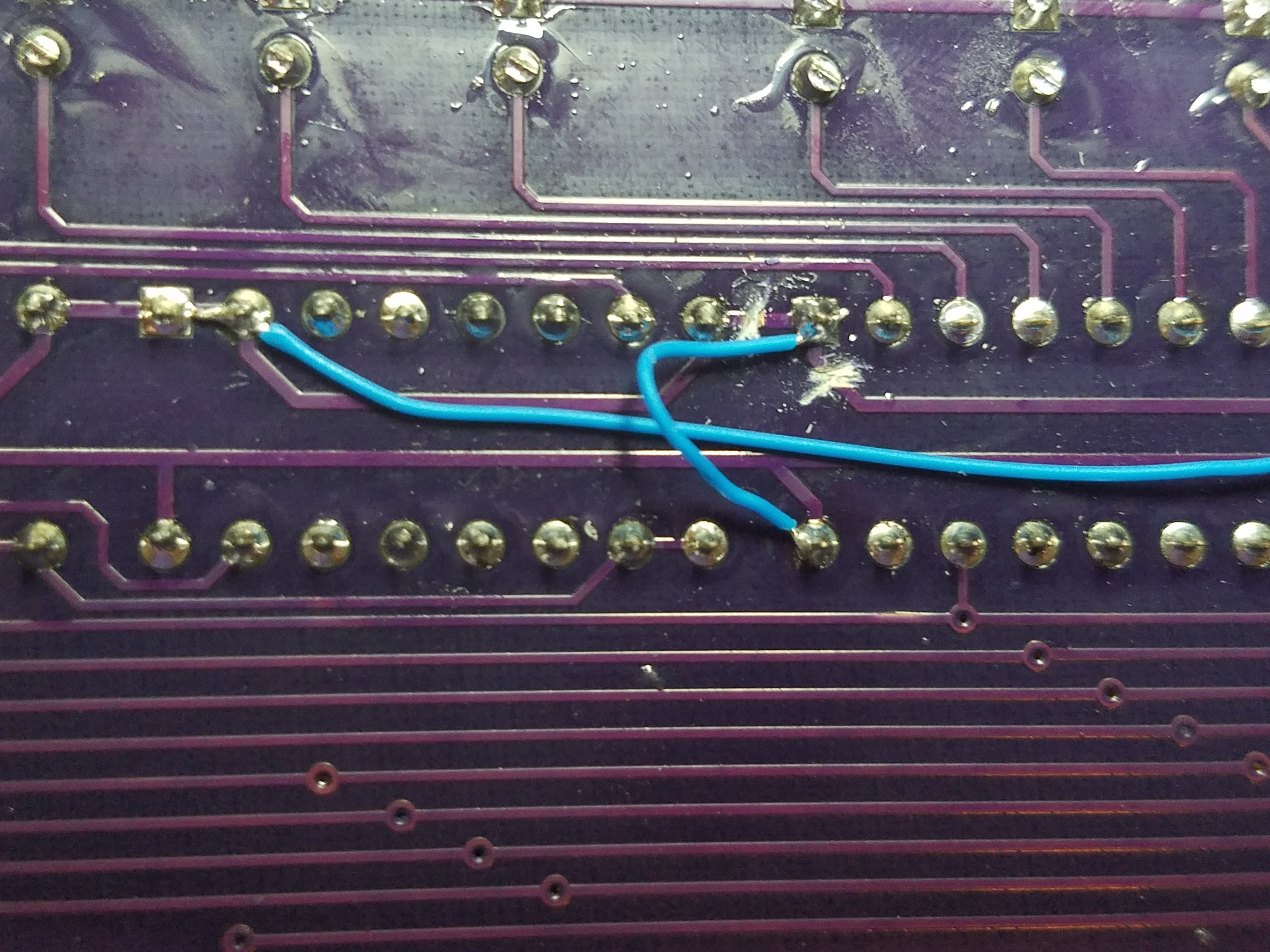
I did come across a design flaw while testing this. I had the direction pin (pin 1) of the 74ls245 set to the wrong value. Because it was set to logic zero (GND), it was expecting to move data from the W Bus to the A Bus when really we need the opposite to happen. The fix was relatively easy, a matter of cutting a couple of traces on the back of the board with an Xacto knife and soldering wire wrap wire to complete new traces:
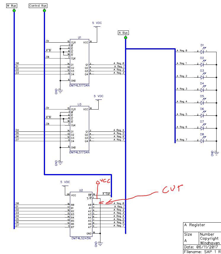
And here is the schematic showing the fix:
And finally, in case you're interested, here is the step two video.
Discussions
Become a Hackaday.io Member
Create an account to leave a comment. Already have an account? Log In.