 agp.cooper
Monitor Time
Time to code the monitor program. Too late to use simulate RAM (unless I have no choice and even then a Nano does not have enough output pins), it is about getting the code to work first time. Yes, well if I am lucky! To help I will write the same monitor code is Pseudo C Code and as commented machine code.
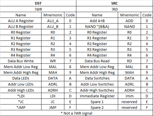
OpCodes
Here are the updated OpCodes:
The main risk is that JC is JNC so I will double check:
It looks okay, a !JC (low) and a CARRY (high) forces !LOAD low.
Subleq Emulator
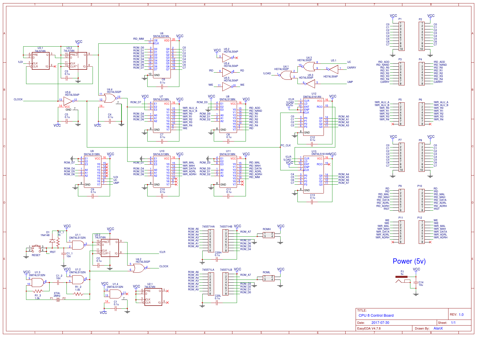
Started writing the emulator, its starting to get complicated with an 8 bit data bus and a 16 bit address space.
The programming of the PROM needs a rethink! The Nano does not have enough output pins to emulate/control the CPU and the micro-code is too big to get right the first time.
I think the immediate objective is to prove the CPU works rather than get the CPU working to final specifications. In order of complexity:
- An 8 bit counter.
- A 16 bit counter.
- A 24 bit counter
- A front panel but no emulator.
Here are the codes for the options:
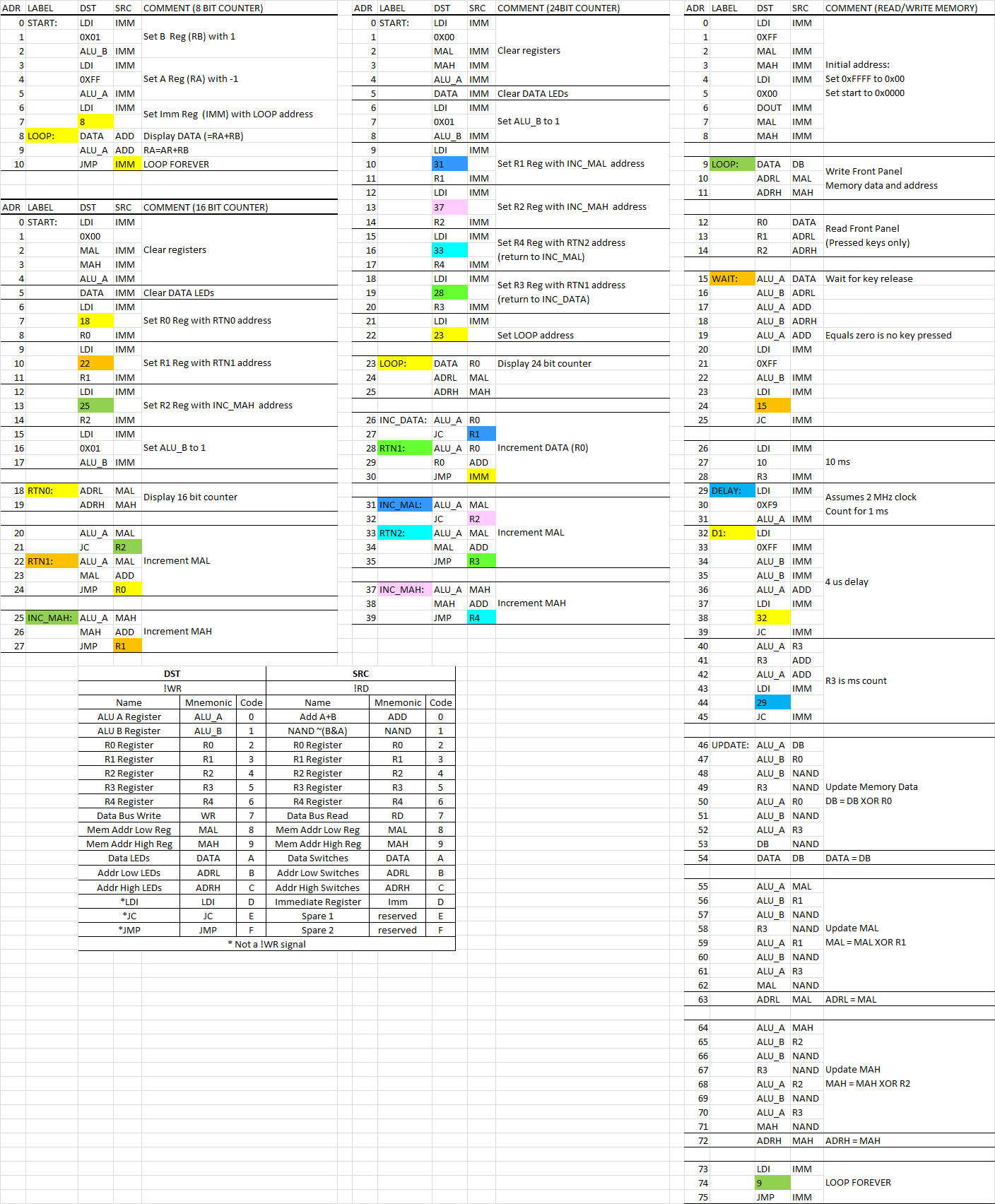
The cut down monitor code looks good to me. It is code I have spend some time working with. A successful run is all I want as the Control board needs to be rebuilt.
The next version of the control board will support a Flash PROM and a way of programming in-circuit. I will replace the Flash ROM with the TTL PROMs when all debugged (want to stay with the TTL style).
Micro Code
Now that I have worked out how to construct simple call/return (see the 16 and 24 bit counters), coding the CPU is more pleasant. I hate using JC when I need JNC (using JC and JMP) as it takes six instructions instead of three if using immediates). It can be done but I will lose a register. Pleasant coding is winning at the moment.
In Circuit Programming of the Flash Memory
Rather than use two PROM which have to be programmed in a specially designed programmer, I want to in-circuit program a flash memory chip.
I can do this by isolating the flash chip with series resistors. Currently the PROMs have:
- one LS-TTL output to the PROM address bus (i.e. 74LS161s)
- 2-3 inputs reading the PROM data bus (i.e. 74LS138s).
Standard LS-TTL Specifications:
- VIL 0.8v max
- VIH 2.0v min
- VOH 2.7 min (3.4 typ)
- VOL 0.5v (max) (0.35 typ)
- IIL 0.36mA
- IIH 20uA
- IOL 8mA
- IOH 400uA
Case 1 Resistors
The value resistor is 1.2k:
- 6.5k = (3.4 - 0.8) / 400u (output high)
- 1.2k = (0.8 - 0.35) / 0.36m (output low)
The datasheet is rather conservative. Measurements suggest 0.20mA rather than 0.36mA (consistent with the LS-TTL schematic showing an 18k to 20k internal pull-up resistor). The maximum resistor in this case is 2.2k. To be safe I will use a 1.8k resistor.
The programming current (I1) from the Adruino would be 2.6mA (=(0.8v - 0.3v) / 1.8k).
Case 2 Resistors
Same as above but 1/3 of 1.8k (or 630R) .
The programming current (I2) from the Arduino would be (when the output is an input) -800uA (to the Arduino). Enough to pull down 4 gate inputs (at 200uA per gate) (=(0.3v - 0.8v) / 630).
Here is the schematic of the in-circuit flash RAM:
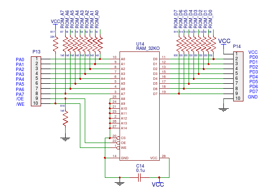
No it will not work! Here is another version:
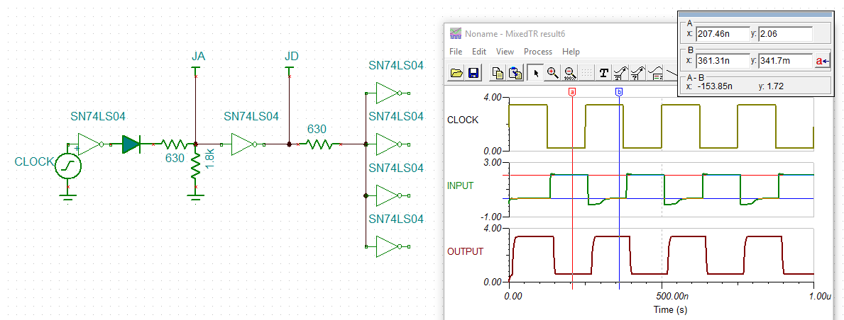
JA is the Arduino Address and JD is the Arduino Data. The first 74LS04 will have to source up to 4.8 mA. As the input low current is only 10uA for the Flash RAM I can increase the input resistor values network up to 20 times. This circuit pull 640uA from the output:
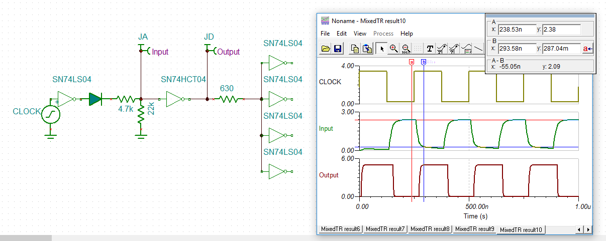
All good now!
The Plan
The plan now is to:
- Code the 16 bit counter in one page of the PROM
- Then the demonstration monitor in the other page of the PROM.
- If all good then a new set of boards using a smaller footprint and the Flash RAM.
I have already redesigned for JNC and JC conditional jumps.
A Stack
What this CPU needs is a stack. The first version is a short (8 bit) stack:
/*
 * PUSH R0
 *    CALL WITH "JMP IMM" AND RETURN WITH "JMP RTN"
 *    SP = R3
 *    RTN = R2
 *    SP = SP - 1
 *    MEM[SP] = R0
 *    RA AND RB DESTROYED
 *    17 INSTRUCTIONS
*/
DST   SRC
===   ===
//    DECREMENT SP
LDI   IMM
0XFF
RB    IMM
RA    SP
//    SWAP MAL AND SP
SP    MAL
MAL   ADD
//    SAVE MAH IN RA
RA    MAH
//    SET MAH
MAH   IMM
//    PUSH R0
DB    R0
//    RESTORE MAH
LDI   IMM
0X00
RB    IMM
MAH   ADD
// SWAP MAL & SP
RA    SP
SP    MAL
MAL   ADD
// RETURN
JMP   RTN
/*
 * POP R0
 *    CALL WITH "JMP IMM" AND RETURN WITH "JMP RTN"
 *    SP = R3
 *    RTN = R2
 *    MEM[SP] = R0
 *    SP = SP + 1
 *    RA AND RB DESTROYED
 *    19 INSTRUCTIONS
*/
DST   SRC
===   ===
//    SWAP SP & MAL
LDI   IMM
0X00
RB    IMM
RA    SP
SP    MAL
MAL   ADD
//    SAVE MAH IN RA
RA    MAH
//    SET MAH
LDI   IMM
0XFF
MAH    IMM
//    POP R0
R0    DB
//    RESTORE MAH
MAH   ADD
//    INCREMENT SP
LDI   IMM
0X01
RB    IMM
RA    MAL
// SWAP SP AND MAL
MAL   SP
SP    ADD
// RETURN
JMP   RTN
A short stack and two free and one temporary registers seems to be all you need.
Another model is a full 16 bit stack with an 8 bit index (i.e. no free registers). In this case all operations use the stack. This model would be best for a simple compiler using P-Code or similar.
Some More Next Version Improvements
Now that I have written a short stack procedures for Push and Pop, I looks like I will move straight to an OpCode CPU.
With the last version of the Push and Pop subroutines, I called them with a call using the IMM (immediate) register and return using RTN (or R2).
I used R3 for the SP. That left me with R0 and R1 free. (R4 was given up for JNC OpCode.)
In order to shuffle around the registers (MAL/SP and MAH mostly) I had to use the ALU for temporary storage. It occurred to me that I could use two of my three spare read slots to read the A and B registers of the ALU, making using the ALU to temporarily store data more efficient (just two extra chips but less one for R4).
So ow my new CPU model would be:
- RA (ALU A Read/Write Register)
- RB (ALU B Read/Write Register)
- R0 (General Read/Write Register)
- R1 (General Read/Write Register)
- RTN (Return Address Read/Write Register)
- SP (Short Stack Pointer Read/Write Register)
- MDB (Memory Data Bus Read/Write Memory)
- MAL (Memory Address Low Read/Write Register)
- MAH (Memory Address High Read/Write Register)
- DATA (Write Data LEDs and Read Data Switches)
- ADRL (Write Address Low LEDs and Read MAL Switches)
- ADRH (Write Address High LEDs and Read MAH Switches)
- lLDI/IMM (Load Immediate Data/Read Immediate Register)
- JNC (Write Jump on Not Carry and Read ALU ADD)
- JC/NAND (Write Jump on Carry and Read ALU NAND)
- JMP/SpareInput (Write Jump and Read Spare)
The (micro-code) Call and Return takes 6 instructions to set up and one to return.
The Push subroutine currently takes 16 instruction excluding the return
The Pop subroutine currently takes 18 instruction excluding the return
Lastly, I coded the SP top as 0xFF00. I think this should be set to 0X0200. The first instruction would just jump over it. I think the 6502 is set up this way.
---
This is stating to get exciting!
AlanX
Discussions
Become a Hackaday.io Member
Create an account to leave a comment. Already have an account? Log In.