Close
0%
0%

HDL training board by FPGA for real beginner

Previously I've made CPLD board, but eventually new FPGA version!

Similar projects worth following
From view point of user experience, CPLD and FPGA (with flash) are almost identical just for writing HDL. But recent FPGA has several built-in module such as I2C and SPI and it leads to good possibility to make "original I2C chip" or "original SPI chip". This time I made a FPGA training board by Lattice's MachO2-256, which has both I2C and SPI "ready-made" module inside and suitable for such purpose. I know the vendor (Lattice) has a product of "$30 break-out board" but we need to add several SW and LED just for initial testing. This board has embedded programmer by FTDI FT232HL, five tactile SWs, two 7-seg LEDs and one buffer amp for Piezo sounder. As same as my previous Xilinx 9572XL based board, this board as very low frequency time base, from 8 Hz (not kHz) to 2048 Hz and those are injected to FPGA. This board is not for professional but beginner. This board has good possibility...!

NEWS

Now this board is available at my tindie store!!


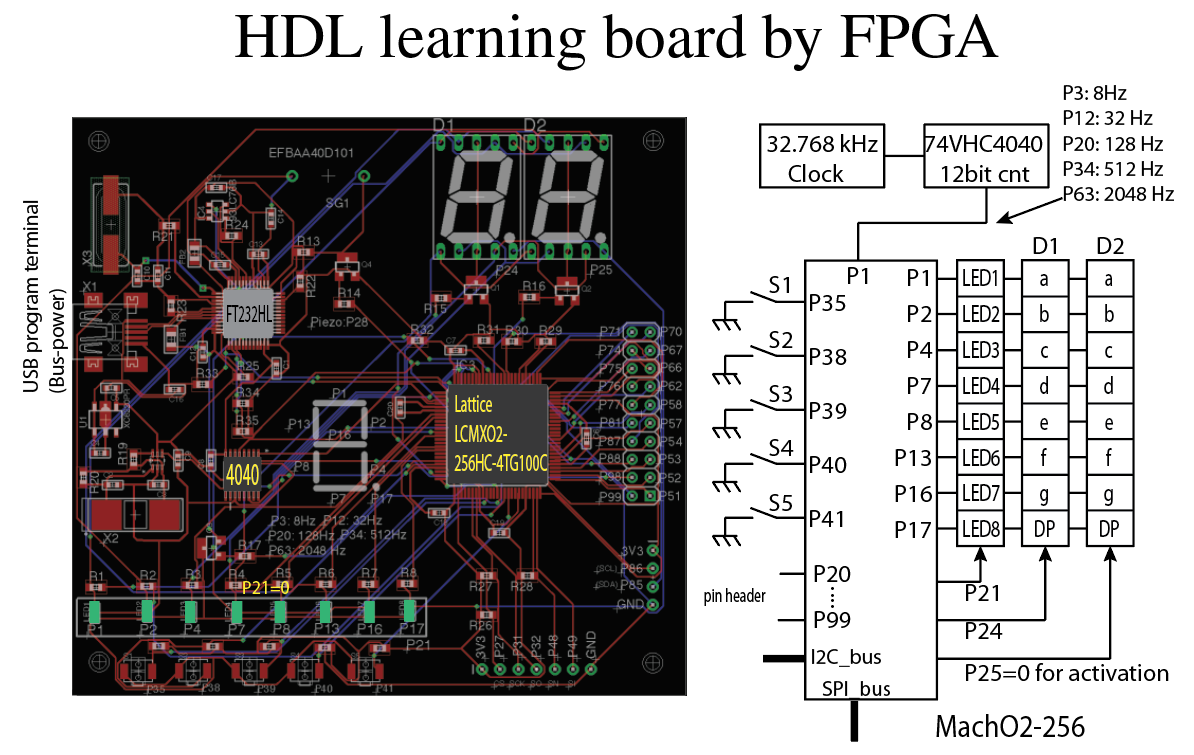
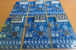
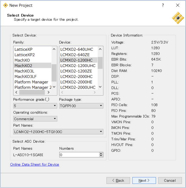
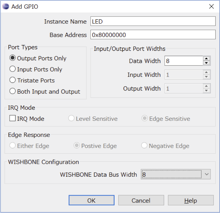
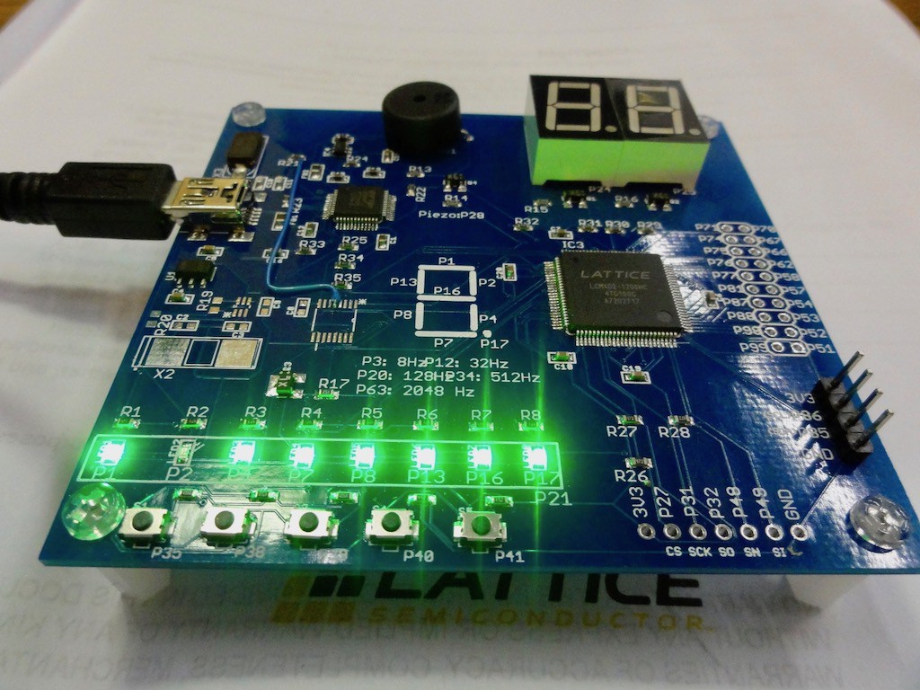
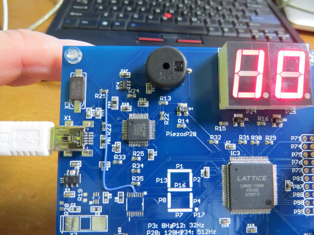
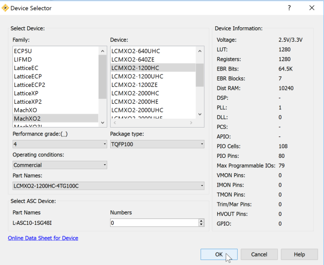
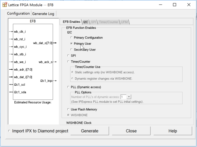
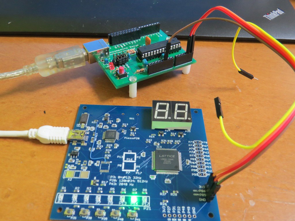
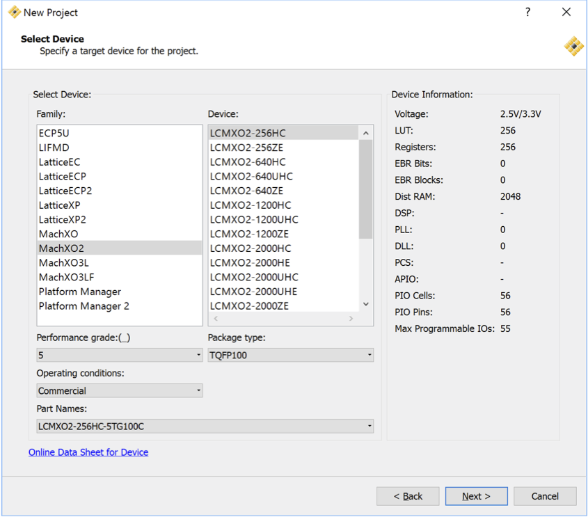
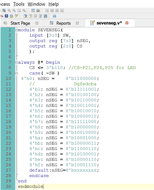
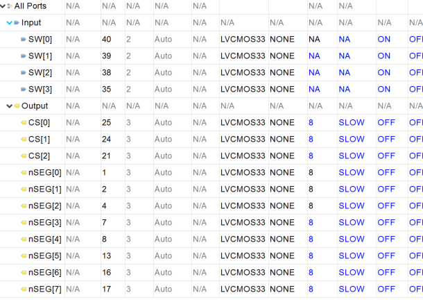
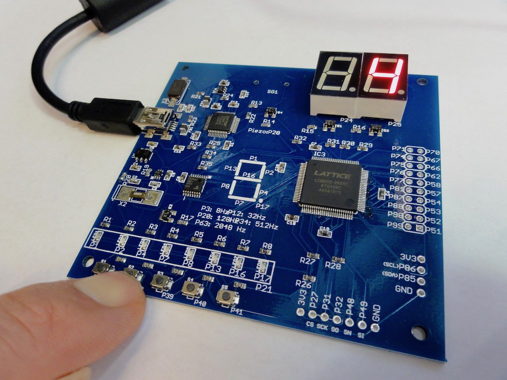
This board is a kind of revised version of my previous project but has more remarkable feature by Lattice MachXO2 FPGA. The FPGA in this board (LCMXO2-256HC) is not big but just 256 logical unit but it has "ready-made" I2C and SPI module! On this board, LEDs (just chip diodes and 7-seg LED) are connected through P1 to P17 in bus-fashion and each components can be activated by P21, P24 and P25. As same as previous one, very slow clock from 8 Hz to 2048 Hz are connected to P3, 12, 20, 34, 63 and we can check "hello world" in HDL description.

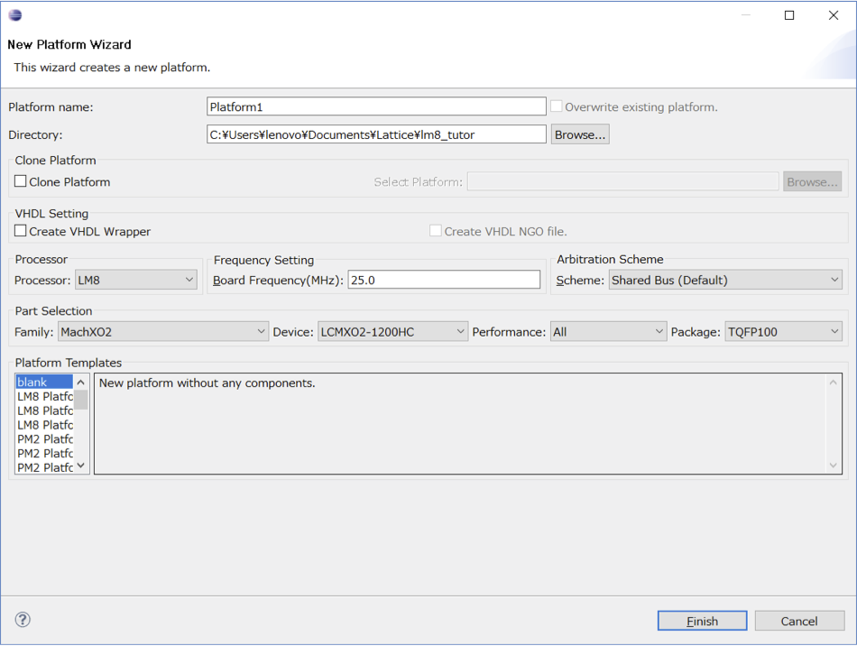
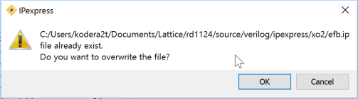
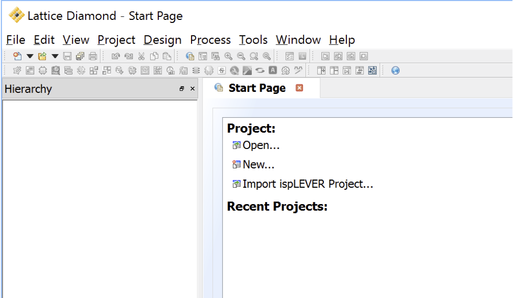
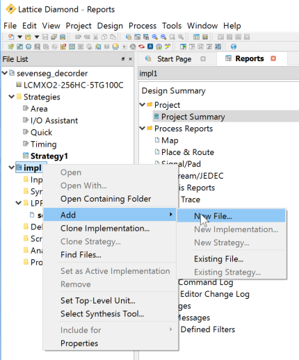
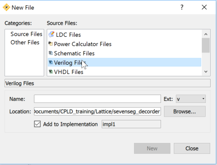
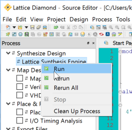
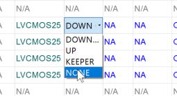
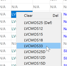
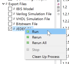
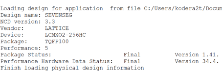
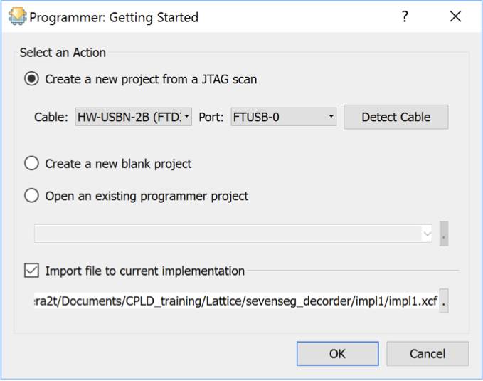
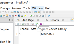
One very remarkable point to previous one is, FPGA programmer on this board is compatible with Lattice Diamond software, which is standard developing environment delivered by Lattice for free of charge. (needs registration). So everything (write, synthesize, upload) can be done within Lattice Diamond. More details (how to program this board) will be released on project log and please refer them...

  • Quick sound generation by Mico8 on MachO2

    kodera2t08/23/2017 at 02:32 0 comments

    Now Mico8 is successfully implemented on the board. Quick change of logic level at GPIO will produce sound and I made a quick check of "sound generation"

    On this board, it is really easy to do it because P28 is connected to piezoelectric sounder through transistor buffer. I just swap MSB of GPIO to piezo out as above.

    Code for Mico8 is also very easy. Just fast switching MSB of GPIO (between 0x7F and 0xFF) is enough to make "game shooting sound"... Have fun!

  • Quick check of Mico8, a 8 bit software CPU on Lattice MachXO2

    kodera2t08/22/2017 at 09:11 0 comments

    Lattice has provided ready-made software processor named Mico8 (8bit CPU) and Mico32 (32bit CPU). This time I quickly checked its developing flow on my board.

    The Lattice's tutorial, which can be available by googling "Mico8 tutorial" is enough to see the fundamentals but some part of this document is out-of-date and we need to swap some words to the new ones.

    In addition to Lattice Diamond, we need to download/install "LatticeMico System for Diamond"


    Here I would like to write just for different point to the tutorial for running on my board.


    The default of the device is not TQFP100 and  just need to select TQFP100 for package type.


    The tutorial says "launch Lattice Mico System" but it is renamed by LMS 1.0


    New Platform wizard at LMS, we should choose LCMX02-1200HC TQFP100


    The board has 8-LEDs so we can add data width to 8.


    Default source of "LM8_LEDTest.c" access only lower 4bit so we need small change to iValue limit.


    In the platform1_top.v, we need to prepare 3bit LED_CS lines and lower bit should be zero for 8-led access.


    On the pinout definition, we need to add and modify as above (3.3V logic, reset pull-up,, cs definition)


    That's all! You will see LED blinking from LED1 to 8! Most interesting point is, the program written by C.

    while(1){
    		MICO_GPIO_WRITE_DATA_BYTE0 (leds->base, iValue);
    		MicoSleepMilliSecs(100);
    		if(iShiftLeft == 1){
    			iValue = iValue << 1;
    			if(iValue == 0x80){
    				iValue = 0x40;
    				iShiftLeft = 0;
    			}
    		}else{
    			iValue = iValue >> 1;
    			if(iValue == 0){
    				iValue = 0x02;
    				iShiftLeft = 1;
    			}
    		}
    	}

    This code is running on a system consisting of CPU, memory, GPIO and the system is fully re-configurable. Just put GPIO module and uploading bitstream, we can make "system". On the same system if we need to change program, just change C-program with same system configuration is enough.... 

  • Quick sound check of FPGA board

    kodera2t08/16/2017 at 09:07 0 comments


    The FPGA board has a piezo sounder connected to P28 of MachO2 through transistor buffer. This time I did a quick check of it by "fast switching" GPIO of FPGA. Still this FPGA is working as a I2C GPIO extender and controlled by Arduino, but also FPGA standalone sound application will be possible...

    The Arduino source code (controlling I2C implemented in FPGA) is as follows:

    #include <Wire.h>
    int sevenseg[10]={
    //abcdefgD////negative logic
    0b00000011,
    0b10011111,
    0b00100101,
    0b00001101,
    0b10011001,
    0b01001001,
    0b01000001,
    0b00011011,
    0b00000001,
    0b00001001,
    };
    /////////////////////////////////////////
    void setup() {
      Wire.begin();//starting I2C of Arduino
    ///activating GPIO of Lattice//
      Wire.beginTransmission(0x09);
      Wire.write(0x06);
      Wire.endTransmission();
    //////////////////////////////
    }
    void loop() {
      for(int i=10;i>=0;i--){
      display_LED(i);
      if(i==0){
        sound(3);
      }
      }
    }
    void display_LED(byte num){
      for(int i=0;i<40;i++){
      byte fstdig_reg=0b11111101,secdig_reg=0b11111011;
        byte secdigit=num/10;
        byte fstdigit=num-secdigit*10;
        dig_select(fstdig_reg);   
        Wire.beginTransmission(0x09);
        Wire.write(0x01);
        Wire.write(0x00);
        Wire.write(sevenseg[secdigit]);
        Wire.endTransmission();
        delay(8);
        dig_select(secdig_reg);
        Wire.beginTransmission(0x09);
        Wire.write(0x01);
        Wire.write(0x00);
        Wire.write(sevenseg[fstdigit]);
        Wire.endTransmission();
        delay(8);  
    }}
    void dig_select(byte reg){
        Wire.beginTransmission(0x09);
        Wire.write(0x01);
        Wire.write(0x01);
        Wire.write(reg);
        Wire.endTransmission();
    }
    void sound(int repeat){
        for(int j=0;j<repeat;j++){
          for(int i=0;i<1000;i=i+2){
        Wire.beginTransmission(0x09);//select 0x09
        Wire.write(0x01);//"write GPIO" command
        Wire.write(0x01);//select GPIO_1
        Wire.write(0b11110111);//write GPIO1_3=0 (P28=0)
        Wire.endTransmission(); 
        delayMicroseconds(i);    
        Wire.beginTransmission(0x09);//select 0x09
        Wire.write(0x01);//"write GPIO" command
        Wire.write(0x01);//select GPIO_1
        Wire.write(0XFF);//write GPIO1=0xFF (P28=1)
        Wire.endTransmission(); 
        delayMicroseconds(i); 
        }
        }
    }
    

     Indeed, this is not FPGA training but just writing Arduino sketch but surely confirmed its "sounding" Actual operation can be seen in the following movie..

  • How to enjoy I2C by EFB inside Lattice FPGA?

    kodera2t08/15/2017 at 02:06 0 comments

    !NEWS!

    Now this board is available at tindie store!

    Lattice MachO2 has a wonderful embedded block enables handy I2C device creation. Here I would like to show you how to enable it. Starting from scratch is far beyond my level and let's start from Lattice's reference design.

    (1) Get files from Lattice site

    By googling "RD1124 Lattice" will guide you the download site. Just click zip file and download it.


    (2) Extract zip and place it on your folder


    Inside zip file, it contains "rd1124" and let's put it in, for example document folder


    (3) Open project file


    Inside rd1124 folder, it contains files both for MachXO3 and MachXO2. Let's confirm the file inside project/xo2/verilog. Now execute Lattice Diamond and select the project file...


    (4) Change program device


    The default device is 132pins version but my board is TQFP100 version of LCMXO2-1200HC. Let's change the device by right click on the device name.


    The appropriate selection is shown above. Please don't forget to change package type to TQFP100.

    (5) Source file modification


    The original sample file assume 132pins version and it cannot be fit inside TQFP100 version (lack pins). Let's change values of i2c_gpio.v as above and save file...


    (6) Rerun synthesize by modified verilog file


    On the process tab, right click on "Lattice Synthesis Engine" will create new file along the modification. Just parameter change will not make any error...

    (7) Pin layout definition


    Currently pin layout is not still defined. Click "Spreadsheet View" will show you the layout window..


    First of all, let's change logic level from 2.5V to 3.3V. Multiple selection by shift-click and right click and select "LVCMOS33" will change all of pin logic at once.


    Now input pins can be written as above (along my board connection). Clock is injected to pin 63 in my board but we need to adjust it design by design. Five GPIO input are connected to tactile switch in my board. Just to be noted is pull mode of RST_N. It should be "UP", otherwise it will remain reset.


    And let's define output pins.  In my board, Pins of GPIO_0 (1, 2, 4, 7, 8, 13, 16, 17) are connected to LED bus and 21, 24, 25 are device selection (active low). It will not hurt but let's set them all "NONE" for pull mode.

    (8) Device programming setting


    Let's check "JEDEC file" in Export File and right click to "Rerun". This will not show any error if pinout can be fit inside FPGA.

    Now let's connect board to computer!


    Now let's add "Programming File" by right click and Add->New file and


    Select "Other Files" in categories and name it. The name does not matter, and click "New"


    It will show you device scan selection and just click "OK"


    After certain period, you will see the device scan result. It is yellow but don't need to care about it. Just confirm "File Name" column is not empty but filled as above picture.

    (9) Finally Program!


    Just click "Programmer" and


    "Program" will make your board to be I2C controlled GPIO board!!

    How to configure I2C of EFB??

    The above sample is just using preconfigured I2C block in sample, but of course we can configure them by very quick way.


    From Tools menu, click "IPexpress"


    We can see vast number of wonderful possibility (these functions, not limited to EFB, can be tailored and utilize!) but just click "EFB" and set up Project Path by Browse button.


    The default folder to be set for IPexpress is source/verilog/ipexpress/xo2. Just select Folder and


    name file "efb" and Module Output as "Verilog" and click "Customize"


    You will see confirmation of overwrite. Yes, it means the modification will reflect on the current project. Click "OK"


    We have SPI, Timer/Counter and PLL and Flash memory in addition to I2C!!. Current interest is I2C and it has three types, Primary Configuration, Primary User, and Secondary User. MachXO2 has two I2C block and Primary user is connected to pre-defined pins (86 and 85 for SDA, SCL) but Secondary User can take arbitral pins for SDA/SCL. Let's check only "Primary user" and click...

    Read more »

  • Original I2C device making by EFB

    kodera2t08/11/2017 at 07:03 1 comment

    Lattice MachXO2 has a wonderful buit-in function named "Embedded Function Block (EFB)". It is hard-coded macro function and XO2 and XO3 (and more?) has I2C, SPI, Timer/Counter function. Datasheet of Lattice says we can save more than 500 LUT by using EFB and it will be true because,, when I think by myself to make I2C slave device,,, it will not be impossible but vast of consideration will be required with bunch of LUT.

    This time I've tried to check the operation of I2C EFB and surely confirmed its operation. Indeed my trial is started from RD1124 of Lattice's reference design but FPGA on board is TQFP and we just need reduce the number of GPIO (original is 8 consists of input 4 (each has 8bit) and output 4) down to single input and output for one byte for each.

    During making I've noticed (too late?) that, "very slow clock circuit" is useless for large size FPGA. Currently the board has LCMXO2-1200HC (1280 LUT) and very enough to make long-bit counter even for the case of slow clock is needed. (it WAS very useful for small size CPLD) So, 4040 (12bit counter) with 32.768kHz crystal oscillator is not populated on board.

    One thing we should understand for EFB activation is, EFB is accessed through WISHBONE interface if we want to utilize the data to external GPIO and for this purpose we need to use Mico8, a tiny 8bit processor. It is a software processor but just consume 200 LUT and still 80% is free for additional circuit implementation. Also one thing to be noted is, we need clock for Mico8 operation. In the current board, 12MHz clock signal is extracted from FTDI's oscillator.

    The real operation can be found in the following movie.. have fun!

  • How to write HDL and upload to board by Lattice Diamond

    kodera2t07/31/2017 at 08:00 0 comments

    If we see "commercial standard" of HDL writing environment among FPGA/CPLD providers, we are so happy but unfortunately their programming interface is completely different for company by company. Comparing the case of Xilinx ISE and Lattice Diamond, we still see different experience. Here I would like to show how to write HDL on this board step by step.

    Before starting, we need to download Lattice diamond and get free license. After installing diamond, yeah let's get started!

    Step 1: Make new project


    Selecting proper (32bit or 64bit) version of Diamond, just click will show you start page.


    Let's click "New..." and make and name new project


    The default location is not good one and we can switch to user directory and name project name as we wish and click next..


    We need to select device here. The board has

    LCMXO2-256HC-4TG100C

    which has TQFP100 package and 256LUT. Let's select this device and click next..


    Now it will show you project summary. Here let's add Verilog file!


    Step 2: Write your file!

    On "impl", right click and add "New File" will show you the following...


    If you prefer VHDL, just select VHDL files for source files but the example here will be done by Verilog Files. Put name of verilog file (I named "sevenseg.v" ) and click "New" then editor window will appear.


    Any Verilog file are ok but let's write sample like above. This is seven segment decorder. Please note that, this board is "negative logic", means "active low". The Lattice Diamond will check your code in real time and if something is wrong, you will see some error message at the bottom of window.


    After writing, let's synthesize by right-click "Lattice Synthesis Engine". Switching file list and Process list, just click process tab as below..


    Step3: Let's connect HDL and real world!

    If no error, we can proceed to programmer section. At this moment, we don't have .ucf in Xilinx manner and we need to define pin connection of implementation.


    Click "Spreadsheet View" will show you spread sheet of connection.


    Now let's connect SW[0] to P48 by right click  Pin column and select "Assign Pins..."


    In the right side, we can select Pin and select P48..


    On the board, all interfaces are correctly pull-up or pull-down so please select "NONE" for PULLMODE.


    This board is ruining at 3.3 V so please select "LVCMOS33" for IO TYPE


    The above picture shows the completed setting. Setting has more options but at this moment we don't need to touch (and I need to explore...)


    Now let's prepare the implementation. Check "JEDEC File" export and right click will make files to be uploaded to the board. 


    Step 4: Let's program your board!

    If no error as above, let's click "Programmer" button as below,


    This click will show you the next window,


    If not selected FTDI as cable, please select "HW-USBN-2B" or similar type with FTDI interface. After selecting proper "cable" let's click OK..


    Now the environment will already recognize the board device. Let's click "Program" button. It will find your board and upload implementation to the board and you will see seven segment decorder!


    Welcome to software described circuit world!

View all 6 project logs

Enjoy this project?

Share

Discussions

Similar Projects

Does this project spark your interest?

Become a member to follow this project and never miss any updates